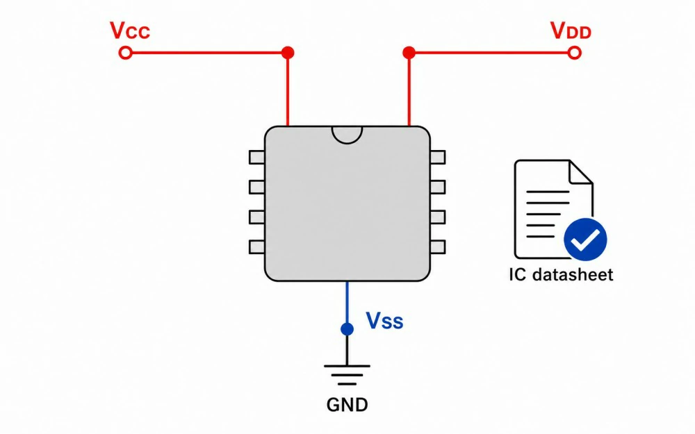
Do not trust the label by itself. Always check the IC datasheet. Look at the pin table, voltage range, exposed pad notes, and power-up rules before PCB layout.
VCC vs VDD vs VSS: Simple Meaning for PCB Designers
Simple Meaning
Important Limit
| Term | Common Meaning | Common Parts | PCB Rule |
|---|---|---|---|
| VCC | Positive supply rail | TTL logic, BJT circuits, interface ICs | Add voltage when needed, such as VCC_5V |
| VDD | Positive supply rail | CMOS ICs, MCUs, sensors, memory | Add function when needed, such as VDD_MCU_3V3 |
| VSS | Lower supply reference | CMOS ICs, MCUs, MOSFET circuits | Check if it connects to GND, AGND, or another node |
| VEE | Negative supply rail | Op-amps, analog circuits, BJT circuits | Do not confuse it with VSS or GND |
VCC Meaning in PCB Design

Original Meaning
Common Voltage Examples
VCC may mean 5V on an older logic board. It may also mean 3.3V on a newer control board. However, the name alone does not show the true voltage.
Clear VCC Net Names
Use a clear name when the board has more than one rail. Good names include VCC_5V, VCC_IO_3V3, and VCC_SENSOR_3V3.
VDD Meaning in PCB Design

Original Meaning
Common VDD Pins
Microcontrollers, memory chips, ADCs, sensors, and RF modules often use VDD pins. A complex chip may have several VDD rails. Examples include VDD_CORE, VDD_IO, AVDD, and DVDD.
Clear VDD Rail Names
VSS Meaning in PCB Design

Original Meaning
VSS in Simple Circuits
VSS in Complex Circuits
For example, a 5V logic buffer may use VCC. A 3.3V microcontroller may use VDD. Do not connect these pins together unless the power tree says they are the same node.

VCC vs VDD Difference
Historical Difference
The main VCC vs VDD difference comes from history. VCC comes from BJT collector supply terms. VDD comes from MOSFET drain supply terms.
Modern PCB Use
Connection Decision
VCC. A 3.3V microcontroller may use VDD. Therefore, these pins should not be connected together unless the power tree says both rails are the same node. VSS vs GND Difference
Basic Difference
Mixed-Signal Boards
This difference matters on mixed-signal boards. An ADC may have AVDD, DVDD, AGND, and DGND. The datasheet may show how these nodes should meet.
Exposed Pad Rules
This difference also matters for exposed pads. A QFN package may need its center pad tied to GND, VSS, or a specific copper area. The package drawing and layout guide should define the connection.
Can VCC, VDD, and VSS Be Interchanged?

VCC, VDD, and VSS should not be interchanged by name alone. Each label describes a power connection, but the real voltage and function depend on the IC datasheet.
Safe Connection Rules
VCC and VDD can sometimes connect to the same positive supply rail. This is only safe when both pins use the same voltage and belong to the same power domain.
VSS often connects to GND in single-supply CMOS circuits. This is not always true in mixed-signal, isolated, or dual-supply designs.
| Question | Short Answer | Safe PCB Rule |
|---|---|---|
| Can VCC and VDD connect together? | Sometimes. | Connect them only when they are the same voltage rail and the datasheet allows it. |
| Can VSS connect to GND? | Usually yes in single-supply CMOS circuits. | Check the datasheet before connecting VSS to the ground plane. |
| Can VSS be a negative rail? | Sometimes. | Review the circuit type before assuming VSS means 0V ground. |
| Is VCC always 5V? | No. | Use names like VCC_5V or VCC_3V3 when voltage matters. |
| Is VDD always 3.3V? | No. | Use names like VDD_3V3, VDD_CORE_1V2, or VDD_IO_1V8. |
PCB Net Naming Rules for VCC, VDD, and VSS
Main Rule
A good power net name tells the reader what the rail does. It should show the voltage, load, or domain when the design has more than one rail.
Good Net Name Examples
- Use
VCC_5Vinstead of onlyVCCwhen 5V matters. - Choose
VDD_MCU_3V3instead of onlyVDDwhen the rail powers the MCU. - Reserve
VDD_CORE_1V2when the rail powers a core domain. - Label
VDD_IO_1V8when an I/O bank uses 1.8V. - Name
AVDD_ADC_3V3when the rail powers an ADC analog block. - Use
PGNDonly when the power ground path is defined.
Example PCB Power Net Names
A small USB sensor board may use USB 5V input, a 3.3V MCU rail, a 1.8V core rail, and a 3.3V analog sensor rail. These names make the design easier to review.
USB Sensor Board Example
| Net Name | Meaning | Why It Helps |
|---|---|---|
VBUS_5V |
USB input supply | Shows the source and voltage |
VDD_MCU_3V3 |
MCU supply | Shows the load and voltage |
VDD_CORE_1V8 |
Core logic supply | Keeps core power separate from I/O power |
VDD_IO_3V3 |
I/O bank supply | Shows the I/O voltage |
AVDD_SENSOR_3V3 |
Analog sensor supply | Shows the analog power domain |
GND |
Main ground | Shows the system reference node |
Datasheet Checks Before PCB Layout
Check Schematic Symbols
The datasheet should guide every power connection. Check the recommended operating voltage, absolute maximum ratings, pin table, decoupling notes, and power sequence.
Check Schematic Symbols
Check every supply pin on the symbol. Some CAD symbols place power pins in a hidden unit. Run ERC checks and compare the schematic with the datasheet pin list.
Check PCB Stackup
Check the layer plan before routing a dense board. A multi-layer PCB stackup guide can help teams plan power planes, ground planes, and controlled impedance traces.
DFM, Assembly, and Test Checks for Power Nets

Fabrication Files
Gerber files show copper shapes. However, they do not explain the power intent. BOM files and Pick and Place files guide assembly, but they do not fix unclear net names.
Assembly Review
Before release, make sure the schematic and PCB layout use the same power nets. Place decoupling capacitors close to IC power pins. Add test points for important rails.
DFM and DFA Review
Power-Rail Testing
Testing should include power-rail checks. AOI can find visible assembly defects. X-ray can inspect hidden joints. ICT or flying probe can check shorts and opens. Functional testing confirms that the board starts correctly. An in-circuit testing overview can help define test needs.
Common VCC, VDD, and VSS Mistakes
Mistakes to Avoid
- Assuming VCC and VDD are always the same. One rail may be 5V, and another rail may be 3.3V or 1.8V.
- Treating every VSS pin as generic ground. Some ICs separate analog, digital, substrate, or exposed pad nodes.
- Using vague net names. A name like
VDD_MCU_3V3is clearer thanVDDon a multi-rail board. - Leaving power pins unconnected. Hidden symbol units can hide supply pins. ERC checks help find this issue.
- Mixing analog and digital rails without notes. AVDD, DVDD, AGND, and DGND need clear connection rules.
- Ignoring exposed pad rules. A QFN or DFN pad may need a specific copper and via pattern.
- Skipping power sequence rules. Some ICs need rails to turn on in a fixed order.
If unclear power nets create a production risk, WellerPCB can review project files for PCB fabrication, assembly, DFM support, prototype builds, and production preparation. Share the schematic, Gerber files, BOM, Pick and Place files, assembly notes, and test requirements through the project contact page.

Conclusion
FAQs
Are VCC and VDD the same
Lorem ipsum dolor sit amet, consectetur adipiscing elit. Ut elit tellus, luctus nec ullamcorper mattis, pulvinar dapibus leo.
Is VSS the same as GND?
Lorem ipsum dolor sit amet, consectetur adipiscing elit. Ut elit tellus, luctus nec ullamcorper mattis, pulvinar dapibus leo.
Why do some ICs use VCC and others use VDD?
Is VSS positive or negative?
Use the clearest name for the design. Voltage names such as 3V3 and 5V are simple. Function names such as VDD_MCU_3V3 are better for complex boards.
What happens if VDD and VSS are connected incorrectly?
The board may fail to power up. The IC may draw too much current or become damaged. Schematic review, ERC checks, and datasheet review should catch this before layout release.
Can DFM review catch VCC, VDD, or VSS mistakes?
DFM review can catch documentation and manufacturability issues. It does not replace electrical design review. The schematic, datasheet, and power tree still control the power design.