Skip to content
  • PCB Layout & Design
    Capability
    • Advantages
    • Design Capability
    • Process
    Solution
    • Reverse Engineering
    • Coplanar Design
    Calculator
    • PCB Trace Width
    • Via Current
    • Impedance
      • Microstrip
      • Embedded Microstrip
      • Edge Coupled Microstrip
      • Stripline
      • Asymmetric Stripline
      • Broadside Coupled Stripline
      • Edge Coupled Stripline
    Learn About
    • FAQ
    • Quote
  • PCB Fabrication
    Capability
    • Multilayer
    • HDI
    • Flex PCB
    • Rigid-flex
    • Process
    • Base Material
    • Surface Finishes
    • Equipment
    • Quick Turn
    Solution
    • DFM
    • Heavy Copper
    • Via in Pad
    • Emdedded Coin
    • Stack up
    • Hybrid PCB
    • Countersink Hole
    • Halogen Free
    • Ionic Contamination
    • Chemical Test
    • IPC Class 2, 3
    • Quality Assurance
    Learn About
    • Altium Designer
    • Eagle PCB
    • Flex
    • PCB Quote
  • PCB Assembly
    Capability
    • SMT
    • Process
    Solution
    • AOI
    • X-ray
    • Firmware & Testing
    • Conformal Coating
    • Encapsulation & Potting
    • Debug & Repair
    • Wire Bonding
    • Underfill
    • Turnkey Solution
    Learn About
    • Quote
  • Our Services
    Engineering
    • Advanced Engineering Services
    Manufacturing
    • EMS
    • Box Build Assembly
    • Rapid Prototyping
    • NPI
    • Cable Harness Mfg. & Assembly
    • CNC Machining
    • Ultrasonic Welding
    • Prototype Molding
    • Injection Molding
    • 3D Printing
    Supply Chain
    • Solutions
    • In Stock
  • Products
  • Case Studies
  • About Us
    • About Weller
    • Why Us
    • Agent Wanted
    • Compliance
    • Warranty
    • Terms & Conditions
      • Standard Terms
      • Supplier Terms
      • Supplier Quality Requirements
      • Specification for Printed Circuit Boards
      • Conflict Minerals Policy
    • Testimonials
    • Holiday Shipping Schedule
    • Latest Blogs
  • Contact
Quote
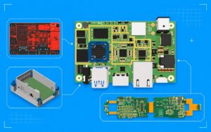
Advanced PCB layout showing PCB design, enclosure integration, rigid-flex circuits, and multi-board assembly

15 Advanced PCB Layout Tips for Complex, Multi-Variant Designs

November 19, 2026

Advanced PCB layout becomes more challenging when products involve multi-board assemblies, rigid-flex circuits, mechanical interfaces, and multiple hardware configurations. Beyond routing and component placement, engineers
Read More »
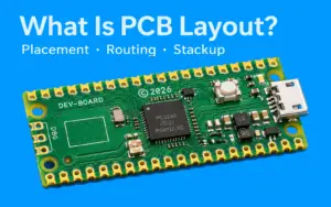
PCB layout illustration showing a green circuit board with component footprints, copper traces, and connectors.

What Is PCB Layout? Definition, Process and Key Design Elements

November 5, 2026

PCB layout turns a verified schematic or netlist into the physical arrangement and interconnection of a printed circuit board. It defines component footprints, placement, copper

Read More »
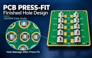
PCB with Würth Elektronik 7461094 press-fit terminals and a magnified inset showing damage around the press-fit holes.

Press-Fit PCB Hole Size and Validation: 1.45 mm vs 1.475 mm

October 23, 2026

The dimensions of PCB press-fit holes directly affect the quality of component press-fit connections, as well as the electrical performance and reliability of the entire

Read More »
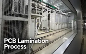
PCB lamination production line with a blue circuit-pattern background and the title “PCB Lamination Process.”

What is the PCB Lamination Process? Steps, Cycles & Common Defects

October 16, 2026

PCB lamination is a key step in multilayer PCB manufacturing process because separately patterned inner-layer circuits must be bonded into one board, with electrical insulation

Read More »
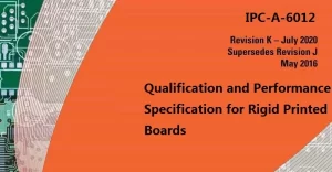
IPC Class 2 and Class 3 rigid PCB manufacturing requirements under IPC-6012

IPC Class 2 & Class 3 PCB Manufacturing: Requirements, DFM & Verification

October 10, 2026

Engineering guide to IPC Class 2 and Class 3 rigid PCB manufacturing, including DFM, plated holes, annular ring, inspection, verification, and procurement requirements.

Read More »
8-layer PCB stackup design example showing typical layer arrangement with signal, ground, and power planes

8-Layer PCB Stackup Design Guidelines: Best Practices & Reference

October 10, 2026

Discover essential 8-layer PCB stackup design guidelines, including best practices, reference layouts, and typical layer configurations shown in diagrams. Learn how to optimize signal and power integrity in multi-layer PCB designs.​

Read More »
« Previous Page1 Page2 Page3 Page4 Page5 Page6 Next »
Tags
Conformal Coating design for manufacturing DFM. Electronics Engineering Electronics Manufacturing Electronics Manufacturing Services ENIG flex PCB HASL HDI PCB high-density interconnect High-Speed PCB high-speed PCB design Impedance Control IPC-2221 Multilayer PCB PCB-Design PCB-Layout PCB Assembly PCB basics PCB Design PCB Design Rules PCB DFM PCB Fabrication PCB Layout PCB Legend PCB Manufacturing PCB materials PCB reliability PCB schematic design PCB Silkscreen PCB Stackup PCB Stackup Design PCB Surface Finish PCB testing Printed-circuit-board Quality Control RF PCB RF PCB design rigid-flex PCB S1000HB Prepreg Signal Integrity SMT assembly Thermal Management Trace Width Calculation
Complete Project

Contact Us Now for Immediate Project Assistance

Address

CN: 4/F, Bldg.3, Huafeng Longgang Overseas Returnees Ind. Park, Baolong lst Rd, Nanyue Cmty, Baolong St, Longgang Dist., Shenzhen, China. 518116

US: 407 Flemington Road,Huntsville,AL 35802, U.S.A.

EU: Z.A.Buisson de la Couldre 8, allée des Châtaigniers 78190 Trappes France.

Phone

+86 755 2828 2776

Email

[email protected]

Make a Request
Drag & Drop Files Here (dsn, pdf, xlsx, dxf, zip, rar up to 8M)
or
Browse Files

WELLER is an Electronic Manufacturing Services provider that specializes in high density Printed Circuit Board Design/Layout, high quality PCB Manufacturing & Assembly and Cable & Wire-Harness. We provide global solutions for seamless migration of customer’s design with our full turnkey services. As a technology-based company, we strive to meet our customer’s electrical, electronic manufacturing and injection molded plastics needs.

PCB Technology

  • PCB layout
  • Manufacturing Capability
  • DFM Analysis
  • HDI PCB
  • Base Material
  • Surface Finishes
  • Embedded Copper Coin
  • Reverse Engineering

PCBA Technology

  • Assembly Capability
  • Firmware Burn-In & Testing
  • Conformal Coating
  • Wire Bonding
  • Underfill Techniques
  • Potting & Encapsulation
  • Debug & Repair
  • Box Build Assembly

Company

  • About
  • Blog
  • Testimonials
  • Warranty

Legal

  • Terms of service
  • Privacy policy
Copyright © 2026 Weller Technology Co. Ltd. All rights reserved.
DMCA.com Protection Status
Linkedin Facebook