PCB lamination is a key step in multilayer PCB manufacturing process because separately patterned inner-layer circuits must be bonded into one board, with electrical insulation between the conductive layers. A conventional double-sided PCB, by contrast, has circuitry on the two faces of a single copper-clad laminate and normally does not require an additional multilayer lamination step during board fabrication. The copper-clad laminate itself has already been manufactured by a laminate supplier such as Shengyi, kingboard, etc.
The PCB lamination process bonds inner-layer cores, prepreg and copper foil using controlled heat, pressure and usually vacuum. During pressing, the prepreg resin flows around the inner-layer circuitry and cures, creating the mechanical bond and electrical insulation between layers. Depending on the stackup and via structure, the board may be bonded in one multilayer lamination cycle or built through sequential lamination stages.
The press cycle also influences dielectric thickness, layer registration, flatness and reliability. This guide explains PCB lamination materials, conventional multilayer bonding, sequential HDI buildup, equipment, process controls and the quality checks designers and buyers should review before production.
What Materials Are Used in PCB Lamination?
A conventional rigid multilayer stackup combines three main materials:

- Core: A fully cured insulating laminate, commonly glass-reinforced epoxy, usually supplied with copper on both sides. Inner-layer circuits are patterned before final multilayer bonding.
- Prepreg: Glass reinforcement impregnated with partially cured resin. During pressing, the resin softens, flows, fills spaces around circuitry, and cures.
- Copper foil: Conductive foil used to create additional circuit layers, commonly the outer layers in a foil-based construction.
The material combination must provide enough resin to fill the copper topography while maintaining the required insulation. Heavy copper, sparse copper areas, and uneven copper distribution make this balance more demanding.

The final dielectric thickness depends on the selected construction and pressing behavior. Designers should use the fabricator’s approved pressed thickness for impedance calculations, rather than assuming an unpressed prepreg thickness will remain unchanged. See WellerPCB’s PCB Prepreg vs Core guide for related material selection considerations.

PCB Lamination Process: Step by Step
Step 1: Review the stackup and manufacturing route
Before releasing production, the board house engineering team confirm layer sequence, laminate and prepreg grades, copper weights, finished thickness, impedance requirements, and via structures. This review determines whether the board can be bonded in one multilayer cycle or requires sequential processing.

Step 2: Prepare and inspect the inner layers
Step 3: Control moisture and lay up the materials
Step 4: Load the press and evacuate air
The layup is assembled with the specified tooling plates, release materials, and pressure-distribution materials. Vacuum helps remove trapped air before the resin gels. Its effectiveness depends on timing, sealing, and the construction being pressed.
Step 5: Heat, consolidate, and cure
Step 6: Cool and verify the panel
Does PCB Layer Count Determine Lamination Cycles?

No. Layer count describes the number of conductive layers; lamination count describes the manufacturing sequence used to bond them.
| Construction | Typical bonding route | Main consideration |
|---|---|---|
| Conventional 4–8 layers, through-holes | Often one multilayer cycle | Material, resin fill, registration |
| Conventional higher-layer-count PCB | May still use one cycle | Heat transfer, alignment, stackup complexity |
| 1+N+1 HDI | Central section plus one buildup stage per side | Microvia formation and central-section preparation |
| 2+N+2 HDI | Central section plus two buildup stages per side | Repeated bonding and via processing |
| Rigid-flex PCB | Construction-dependent | Coverlay, bondply, flex windows, resin flow |
Example: Three Laminations for an 8-Layer 2+4+2 HDI PCB
- First lamination: L3–L6. Build the four-layer central subassembly. Required internal interconnections are drilled and plated before the next buildup stage.
- Second lamination: L2–L7. Add L2 above L3 and L7 below L6. Form and metallize the specified first-stage microvias, such as L2–L3 and L7–L6.
- Third lamination: L1–L8. Add L1 and L8. Form the second-stage microvias, such as L1–L2 and L8–L7, and complete the remaining circuit processing.
If the design also specifies a plated through-hole from L1 to L8, it is mechanically drilled and plated after the full eight-layer stack has been laminated. That through-hole does not itself add another lamination cycle.

What Equipment Is Used for PCB Lamination?

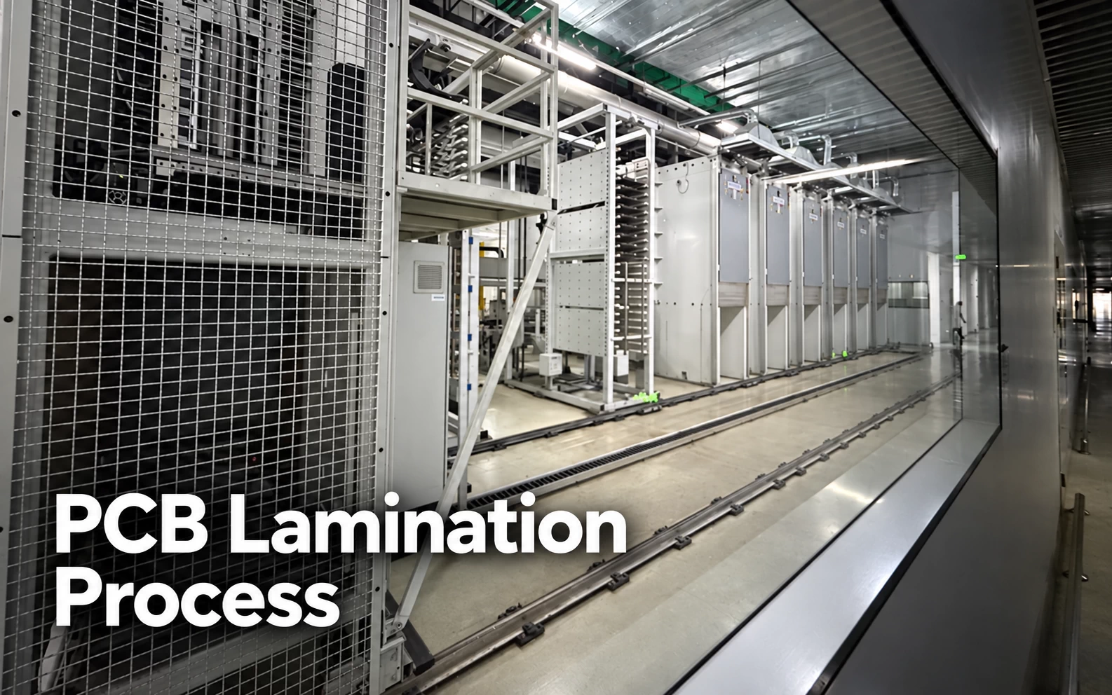
BÜRKLE supplies PCB lamination systems that integrate hydraulic vacuum pressing and heating/cooling functions. WellerPCB’s lamination workshop uses equipment from Germany’s Robert Bürkle GmbH, as documented in our workshop photography. The equipment provides the platform; reliable results also depend on material-specific recipes, maintenance, loading discipline, and verification.
An equipment brand or maximum machine temperature should never be treated as proof that every stackup is qualified. Ask whether the proposed material combination and via structure have an established manufacturing route.
Which Lamination Parameters Matter Most?
There is no universal temperature, pressure, or dwell time for every PCB. FR-4 resin systems, low-loss materials, polyimide-based constructions, and bonding films can require different cycles.
For example, Isola’s FR408HR/HRIS processing guide lists a curing-temperature range of 188–202°C for that material system. This is a material-specific reference, not a general recipe for all FR-4 boards.

- Heat ramp: Influences resin viscosity and the available filling window.
- Pressure and timing: Consolidate the stack without driving out too much resin.
- Vacuum: Helps manage trapped air during the relevant process stages.
- Cure dwell: Must be assessed against actual product temperature and supplier guidance.
- Cooling: Influences dimensional stability and residual stress.
Board thickness, retained copper distribution, and press loading also affect the profile. A qualified recipe should reflect the product construction rather than simply copying settings from another job.
How Is Rigid-Flex PCB Lamination Different?


Common Lamination Defects and Quality Checks
| Issue | Possible contributors | Useful verification |
|---|---|---|
| Voids or incomplete fill | Trapped air, inadequate resin, unsuitable flow conditions | Representative microsections |
| Delamination | Moisture, contamination, poor adhesion, insufficient cure | Bond evaluation and specified thermal testing |
| Layer misregistration | Tooling errors or uncompensated material movement | Registration measurement and X-ray inspection |
| Thickness variation | Resin flow, copper distribution, uneven consolidation | Thickness mapping and sections |
| Bow and twist | Stackup imbalance, uneven processing, residual stress | Flatness measurement |
What to Send for a Lamination Review
Provide Gerber or ODB++ data, drill files, a fabrication drawing, the intended stackup, copper weights, finished-thickness tolerance, impedance targets, material requirements, and a clear via map. For rigid-flex, include flex-region geometry and bending requirements.
PCB Lamination FAQ
1. Why do multilayer PCBs require lamination?
Lamination bonds patterned inner-layer cores, prepreg and copper foil into one board, providing mechanical strength and electrical insulation between conductive layers. Conventional double-sided PCBs normally do not require an additional multilayer lamination step during PCB fabrication.
2. Does PCB layer count determine the number of lamination cycles?
No. Lamination cycles depend on the stackup and via connections, rather than layer count alone. A conventional 12-layer through-hole PCB may require only one multilayer lamination cycle, while an HDI board may require several sequential cycles.
3. Why does sequential lamination increase PCB cost?
Each additional cycle involves further material layup, pressing, via processing and inspection. Repeated thermal exposure also makes dimensional control and layer registration more demanding. The final cost depends on the complete manufacturing route and expected yield.
4. What causes voids or delamination during PCB lamination?
Possible causes include trapped air, moisture, contamination, insufficient resin fill and unsuitable curing conditions. Prevention requires appropriate material handling, surface preparation, vacuum control and a validated temperature and pressure profile.
5. What information is needed to review a PCB lamination stackup?
Provide the layer sequence, material specifications, copper weights, finished thickness and tolerance, impedance requirements, and via connections. Gerber or ODB++ data, drill files and fabrication drawings help the manufacturer confirm the required lamination sequence.