The dimensions of PCB press-fit holes directly affect the quality of component press-fit connections, as well as the electrical performance and reliability of the entire PCBA. In this WellerPCB case, an initial trial showed visible damage, prompting a revised 1.475 mm nominal finished-hole target and validation on two bare boards before SMT. Both samples passed the reported pin-gauge check, with no obvious abnormalities observed after insertion.
These preliminary results support the revised approach for the sampled boards, but do not establish the sole cause of the original damage or replace full process qualification.
1.45 mm vs 1.475 mm: The Original Press-Fit PCB Hole Issue
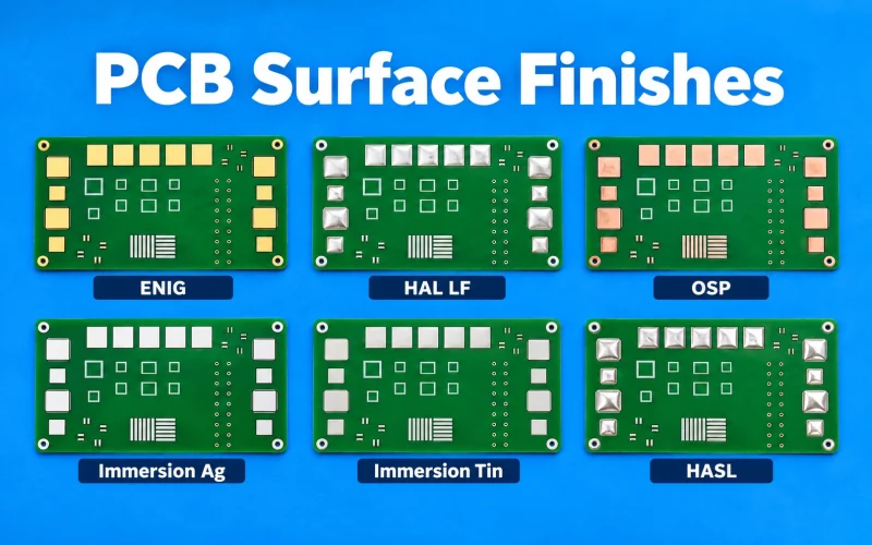
WellerPCB manufactured a four-layer customer PCB with 2.4 mm board thickness, 3 oz copper on all four conductive layers, ENIG with specified gold thickness of 2 µin, and gold-finished plated edges. The assembly incorporated Würth Elektronik 7461094 press-fit terminals. The customer’s stack-up design specified 3 oz copper on all four layers, consistent with the requirements of a high-current application where connection integrity and thermal performance are critical.
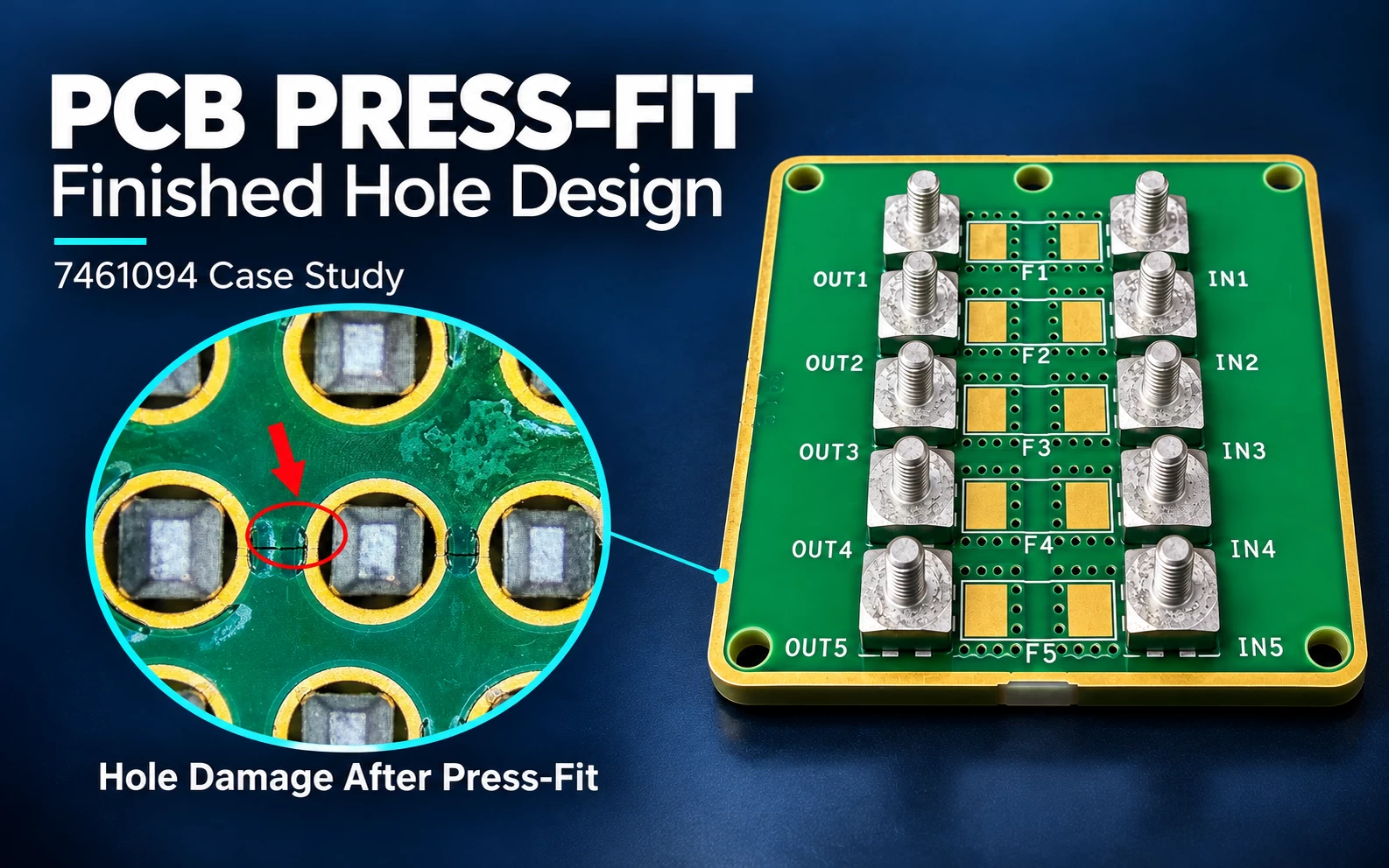
The first trial took place after SMT assembly. Microscopic inspection revealed fractures around the edges of the terminal insertion holes—an unacceptable finding in an assembly using terminals rated at 130 A, where connection integrity is critical. Any damage to the conductive path could increase contact resistance, cause localized overheating, and potentially lead to catastrophic failure.
We traced the issue back through the original PCB design and manufacturing requirements. The customer’s original design specified a nominal finished hole diameter of 1.45 mm for an ENIG-finished PCB.
However, the terminal documentation specified 1.475 ±0.05 mm for chemical finishes, compared with 1.45 ±0.05 mm for HAL.
This discrepancy prompted a revision of the finished-hole target and further verification of the actual hole dimensions, plating integrity, and pressing conditions before proceeding with additional populated boards. Because the two tolerance ranges overlap, the nominal diameter difference alone was not considered sufficient to establish the root cause.
How WellerPCB Validated the 1.475 mm Press-Fit PCB Hole
We shared our findings with the customer, who revised the PCB design to specify a nominal press-fit hole diameter of 1.475 mm. WellerPCB manufactured replacement PCBs and randomly selected two unpopulated boards for dimensional screening and trial press-fitting before SMT. This moved the compatibility check earlier, reducing the risk of discovering a fit problem only after components and assembly labor had been added.
The table below summarizes the checks performed on the two sampled boards, the observed results, and the limits of the validation.
Case Results and Scope of Validation:
| Item | Findings and Evidence |
|---|---|
| Original Issue | Microscopic inspection revealed damage around the terminal insertion holes after the initial press-fit trial. |
| Design Revision | The nominal hole diameter was revised from 1.45 mm to 1.475 mm following a review of the terminal documentation. |
| Validation Samples | Two randomly selected replacement bare PCBs were checked before SMT assembly. |
| Dimensional Check | Both boards admitted the 1.475 mm pin gauge. This check alone did not verify the full hole-diameter tolerance range. |
| Trial Assembly | The terminals were inserted using a press and dedicated support tooling. No obvious abnormalities were reported during the trial. |
| Surface Inspection | No visible cracks were identified in the inspected surface areas after insertion. |
| Scope and Limitations | The results support the revised approach for the two sampled boards. They do not establish the sole root cause, exclude hidden internal damage, or qualify the entire production lot or long-term reliability. |
What the 1.475 mm Pin Gauge Check Establishes
The supplied photographs document the 1.475 mm gauge and checks on the two selected bare boards. WellerPCB reported that both boards admitted the gauge under the inspection conditions.
A 1.475 mm gauge pass alone does not verify the full hole-diameter tolerance.
- A hole above the upper limit may still admit the nominal gauge.
- One nominal gauge cannot independently verify both tolerance limits.
- Do not force a gauge through a plated hole.
Define an approved inspection method for both limits, account for gauge tolerances, and record board identity, sampled locations, gauge identification, and results.
Trial Press Fitting Before SMT
The two bare boards were used for an insertion trial before component placement. The supplied photographs document the press and dedicated support tooling. The purpose of the trial was to assess the revised PCB design and terminal interface before proceeding with the higher-value populated assembly. No obvious abnormality was reported on the trial circuit boards.
Microscope Inspection After Insertion
After pressing, we inspected the accessible areas around the insertion holes with a high-definition microscope. The supplied images show the enlarged board surface and terminal pin regions on the monitor. No visible cracks were identified in the inspected surface areas, consistent with the reported absence of obvious abnormality during the trial.
Surface inspection is valuable for detecting visible pad lifting, cracks, local deformation and seating problems. It cannot demonstrate the absence of concealed barrel cracks, internal delamination or contact defects. Where the application requires stronger evidence, add suitable microsections, retention checks, electrical contact testing and application-specific reliability evaluation. Camera pixel count is not optical magnification; no numerical magnification is assigned to these photographs.
Press-Fit Hole Size: Prepared vs. Finished Holes
| Finish Category | Finished Hole Specification | Acceptance Interval |
|---|---|---|
| HAL | 1.450 ± 0.050 mm | 1.400–1.500 mm |
| Chemical finishes | 1.475 ± 0.050 mm | 1.425–1.525 mm |
These values apply to the cited 7461094 interface, not to all press-fit terminals. The current approved component drawing must govern the project. Copper plating and finish build-up reduce the opening; their variation is part of the fabrication control needed to meet the final dimension.
Why The Nominal Mismatch Is Not A Complete Root Cause
Surface Finish Laminate And Hole Wall Construction
According to Würth Elektronik’s REDCUBE Terminals for High Current Applications (p. 5, “Materials and tolerances”), immersion tin is the recommended PCB surface finish. The document states that ENIG can be used but is not recommended for press-fit technology. For this ENIG-finished PCB, surface-finish suitability therefore required a separate review alongside the finished hole dimensions, hole-wall plating and assembly conditions.
The 2.4 mm board thickness and reported 3 oz layer copper do not remove the need to check hole-wall copper and material compatibility. High-Tg material also requires the manufacturer’s pre-evaluation where specified. Retain the approved laminate, finish and plating requirements with the fabrication release, and verify the manufactured result through the documented PCB manufacturing and inspection process rather than inferring hole construction from outer-layer copper weight.
Suggested Fabrication Note
Fabrication Note — Press-Fit Holes
Finished plated-hole diameter: Ø1.475 ±0.050 mm for the approved chemical-finish configuration used with Würth Elektronik 7461094.
The fabricator must verify the drilling and plating process, hole-wall construction, inspection method, laminate, board thickness, and surface-finish compatibility against the approved terminal documentation before production release.
Identify these critical holes separately from general fabrication tolerances and document the applicable acceptance criteria.
A Practical Release Checklist
- Confirm the exact terminal part number and approved drawing revision.
- Specify the finished diameter, tolerance and surface-finish category explicitly.
- Control hole-wall copper independently of layer copper weight.
- Review hole positions, annular rings, laminate and board thickness.
- Inspect representative finished holes using an agreed dimensional acceptance method.
- Run an early bare-board insertion trial where appropriate and define sample disposition.
- Verify tooling support and clearance again for the populated assembly.
- Record insertion behavior and inspect accessible surfaces after pressing.
- Add internal, mechanical and electrical verification to suit the application.
- Release production using documented acceptance criteria and traceable records, with applicable PCB manufacturing requirements reviewed against the IPC Class 2 and Class 3 PCB manufacturing guide.
Frequently Asked Questions
1. Are press-fit PCB holes manufactured using the same process as standard plated through-holes?
Press-fit holes generally follow the same basic manufacturing steps as standard plated through-holes, including drilling, hole-wall preparation and copper plating.
However, they require specific control of the finished hole diameter, tolerance, plating thickness and surface finish to match the terminal manufacturer’s requirements.
A standard plated hole is therefore not automatically suitable for press-fit assembly. The finished hole size must also be distinguished from the drill tool size used before plating.
The fabricator should control drill-tool condition, drilling parameters and plating variation to achieve the specified finished hole dimensions and hole-wall quality.
2. Do press-fit holes increase PCB manufacturing costs?
They can, but an additional charge is not inevitable. The cost depends on whether the specified hole tolerances and inspection requirements fall within the PCB manufacturer’s normal capabilities. Tighter tolerances can increase fabrication costs. Press-fit assembly may also require dedicated tooling, board support and additional inspection, so the quotation should distinguish bare PCB manufacturing costs from assembly costs.
3. How should press-fit holes be specified in Gerber and fabrication files?
Do not rely on the Gerber copper layers alone. Supply the plated-hole drill data together with a fabrication drawing that clearly identifies the press-fit holes and their requirements. Include:
– Terminal manufacturer, part number and applicable datasheet revision.
– Finished hole diameter and tolerance after plating and surface finishing.
– Hole-wall copper thickness and PCB surface finish.
– Hole positions, positional tolerances and applicable PCB thickness.
Ask the PCB manufacturer to confirm these requirements during engineering review. Clearly distinguish the required finished hole size from the production drill tool size, and require approval before any change to the specified press-fit holes.
4. How are press-fit terminals installed on a PCB?
Align the terminal pins with the specified plated holes, support the PCB beneath the insertion area with a suitable fixture, and use a controlled press with a matching insertion tool. Apply force evenly in the insertion direction, following the terminal manufacturer’s assembly instructions. Inspect the trial assembly for seating, board deformation and damage around the holes before continuing production. Hammering or unsupported pressing should not be used as a substitute for a controlled process.
5. What finished hole diameter is required for Würth Elektronik 7461094?
The 7461094 datasheet specifies 1.475 ±0.05 mm for chemical finishes and 1.45 ±0.05 mm for HAL, together with hole-wall copper requirements. These are component-specific specifications, not universal dimensions for all press-fit terminals. Confirm the applicable surface finish and current manufacturer requirements before releasing the PCB. Because the two diameter ranges overlap, the nominal difference alone does not prove the cause of press-fit damage; actual finished hole measurements and assembly conditions must also be reviewed.