High Tg PCB: Benefits, Materials, Applications, and Design Guide
A High Tg PCB uses a laminate with a higher glass transition temperature than standard FR4. It resists heat better. It keeps its dimensions more stable. It also improves reliability during lead-free soldering, rework, thermal cycling, and long-term field operation. If you design automotive electronics, industrial controllers, telecom equipment, medical devices, LED drivers, robotics systems, […]
Essential PCB Layout Guidelines for High-Performance Electronics Design

In the world of electronics design, a schematic is only half the story. The true performance, reliability, and manufacturability of a product are determined during the PCB layout stage. A well‑executed PCB layout can mean the difference between a product that passes EMC testing on the first try and one that suffers from noise, crosstalk, […]
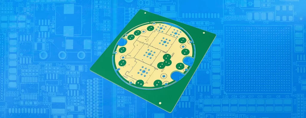
High-Voltage PCB Design: Clearance, Creepage, Slots & Insulation Systems

Modern electronic systems are increasingly required to handle high voltages —from renewable energy converters and electric vehicles to medical imaging systems and industrial automation. Designing printed circuit boards (PCBs) that safely and reliably operate at high voltage levels demands more than standard design rules. A high-voltage PCB (HV-PCB) must prevent arc discharge, dielectric breakdown, and […]
How AI & Automation Are Transforming PCB Manufacturing
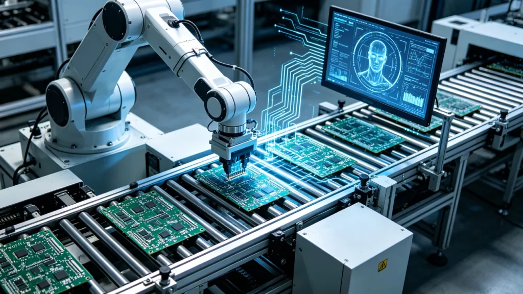
The printed circuit board (PCB) manufacturing industry is undergoing a major transformation. As electronic products become smaller, faster, and more complex, traditional manufacturing methods are struggling to keep up. To meet growing demands for quality, speed, and cost efficiency, PCB manufacturers are increasingly turning to Artificial Intelligence (AI) and automation. AI and automation are no […]
From Prototype to Mass Production: Best Practices for Smooth NPI in PCB Design
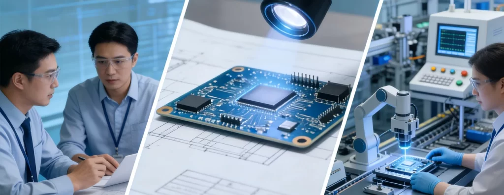
In the electronics industry, building a working prototype is only the first step. The real challenge begins when that prototype must be converted into a reliable, cost-effective product that can be manufactured in large volumes. This transition is known as New Product Introduction (NPI), and it plays a critical role in the success of any […]
Coating vs. Encapsulation: Choosing the Right Protection for Your Electronics
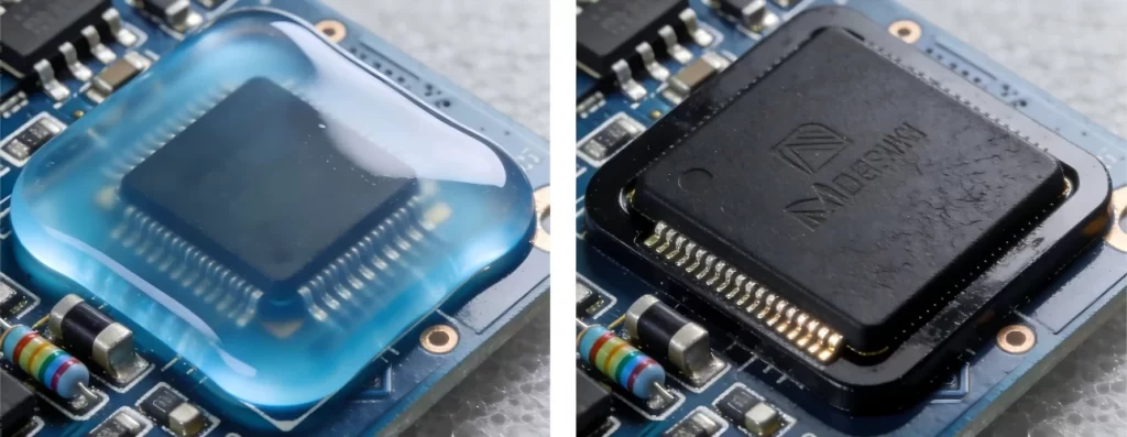
Conformal coating vs encapsulation for electronics is a critical decision for design engineers and product managers developing PCBs for harsh environments. Conformal coating applies a thin polymeric film (25–250 µm) that conforms to board contours, preserving repairability and minimizing weight. Encapsulation (or potting) completely immerses the assembly in a thick resin (millimeters to centimeters), delivering […]