In the world of electronics design, a schematic is only half the story. The true performance, reliability, and manufacturability of a product are determined during the PCB layout stage. A well‑executed PCB layout can mean the difference between a product that passes EMC testing on the first try and one that suffers from noise, crosstalk, or thermal failures.
Whether you are designing a high‑speed digital board, an RF module, or a mixed‑signal IoT device, following proven PCB layout guidelines is essential. This article covers the most critical rules – from software selection and component placement to routing, grounding, and thermal management – and also introduces leading PCB layout service companies around the world that can help bring your design to life.
Why PCB Layout Matters
PCB layout translates a logical schematic into a physical board. It directly impacts:
- Signal integrity – reflections, ringing, crosstalk
- Power integrity – IR drop, decoupling effectiveness
- EMC/EMI – radiated and conducted emissions
- Thermal performance – heat spreading and hot spots
- Manufacturing yield – DFM rules, solderability, testability
Ignoring layout guidelines often leads to costly respins, delayed time‑to‑market, and field failures.
A standard acid copper plating bath typically consists of:
The organic additive system contains three functional groups:
- Suppressor (Carrier): Polyethylene glycol (PEG) molecules that adsorb on surfaces and inhibit deposition in low-field regions.
- Accelerator (Brightener): Thiol-containing compounds promoting copper deposition in high-aspect-ratio vias.
- Leveler: Heterocyclic amines that even out surface roughness and mitigate “mushrooming” at hole edges.
The delicate balance between suppressor and accelerator adsorption determines how uniform copper deposition will be across the hole walls and surface areas.
11 Essential PCB Layout Guidelines
1. PCB Layout Software Selection – Choosing the Right Tool
Before you place a single component or route a trace, you must choose a PCB design software (EDA tool) that matches your project’s complexity, budget, and team collaboration needs. The right tool can dramatically speed up layout, enforce design rules, and integrate with simulation and manufacturing outputs.
Key factors to consider:
- Layer count support – Does the tool handle 2‑layer boards, 16‑layer high‑speed designs, or even 30+ layer HDI?
- Constraint management – Can you set differential pair rules, length matching, and impedance profiles?
- Simulation integration – Built‑in signal integrity / power integrity (SI/PI) or easy export to Ansys, HyperLynx?
- Component libraries – Access to vendor‑supplied footprints and 3D models.
- Team collaboration – Version control, design review features, and cloud sharing.
- Cost – Free open‑source vs. subscription‑based professional suites.
Popular PCB layout software (from entry to expert):
Software | Best for | Typical cost | Key strength |
|---|---|---|---|
KiCad | Hobbyists, startups, open‑source | Free | Free Full feature set, no restrictions |
EasyEDA | Beginners, integration with JLCPCB | Free (cloud) | Direct manufacturing export |
Autodesk Eagle | Makers, small teams | $15‑$100/month | Large community, Fusion 360 integration |
Altium Designer | Professional electronics design | ~$3k‑$6k one‑time + subscription | Unified environment, real‑time DRC |
Cadence Allegro | High‑speed, HDI, telecom, aerospace | High ($10k+) | Industry‑leading constraint manager |
Mentor (Siemens) PADS | Mid‑range professional | $2k‑$5k | Good balance of power and price |
Zuken CR‑8000 | Advanced automotive, aerospace | High | Strong 3D and multi‑board support |
Tip for beginners: Start with KiCad – it is completely free, professionally capable, and has an active community. For professional teams targeting high‑speed designs, Altium Designer or Cadence Allegro are industry standards.
Once you have selected your software, invest time in setting up your design rules (trace widths, clearances, via sizes) and library management before starting layout.

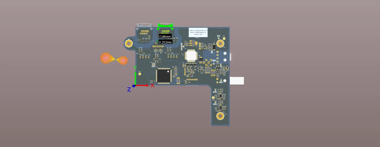
2. Component Placement – The Foundation of a Good Layout
Before routing a single trace, spend 40‑50% of your layout time on placement. Good placement reduces routing complexity and improves signal integrity.
Guidelines:
- Place connectors and mechanical interfaces first (edge of board).
- Position high‑speed ICs (processors, FPGAs, memory) close to their associated interfaces.
- Keep decoupling capacitors as close as possible to IC power pins – ideally within 1‑2 mm.
- Group analog and digital circuits separately; create physical isolation.
- Place noisy components (clocks, switchers) away from sensitive analog or RF circuits.

3. Stackup Design
The layer stackup determines return path quality and impedance control.
Guidelines for typical 4‑layer board:
- Layer 1: High‑speed signals + components
- Layer 2: Solid ground plane (no splits)
- Layer 3: Power plane or secondary signals
- Layer 4: Low‑speed signals + components
For 6+ layers, add additional ground planes adjacent to high‑speed signal layers.
📌 Key rule: Every signal layer must be adjacent to a continuous reference plane (GND or power) to control impedance.
4. Trace Routing Best Practices
- Avoid 90° corners – use 45° bends or arcs to reduce reflections.
- Match lengths for differential pairs (USB, HDMI, Ethernet) and parallel buses (DDR). Typical tolerance: ±5 mils within pair, ±50 mils between pairs.
- Keep high‑speed traces short – place critical components close to connectors.
- Route sensitive signals (clocks, analog) away from noisy lines (power, digital). Use 3W spacing (3× trace width) to minimize crosstalk.
5. Grounding and Return Paths
- Use a solid ground plane whenever possible. Avoid splits under critical signals.
- For mixed‑signal boards, split the ground plane only if absolutely necessary, and bridge the split at a single point under the ADC/ DAC.
- Provide a low‑impedance return path – the return current always follows the path of least inductance, which is directly under the signal trace.
6. Decoupling and Power Distribution
- Place bulk capacitors (10‑100 µF) near power input connectors.
- Place ceramic decoupling caps (0.1 µF, 1 µF, etc.) as close as possible to each IC power pin – use multiple vias to ground.
- For high‑current paths, use thick traces or copper pours and add multiple vias for low inductance.

7. Thermal Management Guidelines
- Add thermal vias under hot components (e.g., voltage regulators, power LEDs) to transfer heat to inner or bottom layers.
- Use copper pours on outer and inner layers to spread heat.
- For very high power, consider copper coins or heatsinks attached to the board

8. High‑Speed Differential Pair Routing
- Keep differential pairs tightly coupled (intra‑pair spacing ≤ 2× trace width).
- Maintain consistent spacing; avoid vias if possible. If vias are necessary, use symmetrical via placement.
- Avoid stubs – route directly from driver to receiver.
9. Via Usage
- Use microvias for HDI designs; for through‑hole vias, keep them away from SMD pads (unless via‑in‑pad is specified).
- For high‑speed signals, minimize via count – each via adds capacitance and impedance discontinuity.
- For power and ground, use multiple parallel vias to reduce inductance.
10. Design for Manufacturing (DFM)
- Follow your fabricator’s minimum trace/space, via size, annular ring, and solder mask clearance rules.
- Add fiducial marks (three globally, one near fine‑pitch components) for SMT assembly.
- Provide clear silkscreen polarity indicators, pin‑1 markers, and reference designators.
11. Verification Steps
- Run DRC (Design Rule Check) – both electrical and physical.
- Perform signal integrity simulation for critical nets (DDR, PCIe, USB).
- Use power integrity analysis to check IR drop and plane resonance.
- Generate Gerber files and review them in a separate viewer.
Global PCB Layout Service Companies
Not every electronics design team has in‑house layout expertise. Many companies outsource PCB layout to specialized design bureaus. Below are notable PCB layout service providers from key regions – USA, Europe, Japan, Korea, Taiwan, and China.
🇺🇸 United States
- Sunstone Circuits (PCB design services) – Offers turnkey layout and prototyping.
- Sierra Circuits – Provides full PCB design, layout, and DFM analysis.
- EMA Design Automation – Specialized in high‑speed and RF la
🇪🇺 Europe
- Würth Elektronik (Design Services) – German company offering layout, simulation, and prototyping.
- Eurocircuits – Known for online ordering and professional layout services.
- Ineltek (UK/Germany) – Design house with strong analog and RF layout expertise.
🇰🇷 Korea
- Samsung Electro‑Mechanics (Design support) – Provides layout services for high‑speed memory and mobile boards.
- Daeduck Electronics (Design center) – Supports customers with full PCB layout and DFM.
🇯🇵 Japan
- Sanyo PCB Design – Provides high‑density and HDI layout services.
- Meiko (Design division) – Offers layout for automotive and industrial electronics.
🇹🇼 Taiwan
- Unimicron (Design service) – Offers layout assistance for advanced HDI and substrate‑like PCBs.
- Compeq Manufacturing (Design support) – Provides layout engineering for mobile and networking products.
- Zhen Ding Technology – Design services for high‑layer‑count and flexible PCBs.
🇨🇳 China
- FastPCB (PCB layout & prototyping) – Rapid turnkey layout and manufacturing.
- Fastprint (Design services) – Affordable layout services for simple to medium‑complexity boards.
- Hampoo PCB Design (Shenzhen) – Specializes in high‑speed, DDR, and RF layout.
- WELLER PCB – Offers professional layout with DFM/DFA analysis.
💡 Tip: When selecting a layout service provider, review their previous work, ask about design rules they support (e.g., 3 mil trace/space), and request a DFM report sample.
Integrating PCB Layout with EMS and Fabrication
A great PCB layout must be manufacturable and assemblable. That is why leading Electronics Manufacturing Services (EMS) providers maintain close relationships with layout design houses. They often offer in‑house layout review as part of their NPI (New Product Introduction) process.
If you are working with an EMS partner, share your layout files (Altium, Cadence, KiCad) early for DFM/DFA feedback. This prevents costly changes later.
Conclusion
Mastering PCB layout guidelines is a continuous learning process. From software selection, component placement, stackup design to routing, grounding, and thermal management, each decision affects the final product’s performance and cost. Whether you do the layout in‑house or partner with a specialized design company, following the guidelines above will reduce risk and accelerate your time‑to‑market.
Ready to start your next PCB layout project? Contact our engineering team for a free layout review or a referral to trusted design partners in your region.


