
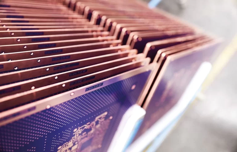
Copper electroplating is the backbone of modern printed circuit board (PCB) manufacturing. From through-hole connections in double-sided boards to microvias in HDI (High-Density Interconnect) structures, proper plating chemistry determines both electrical connectivity and mechanical reliability.
The plating process may appear straightforward — deposit copper onto a conductive surface — but in practice, success depends on solution chemistry, current distribution, additive control, and process monitoring. A poorly managed plating bath can lead to catastrophic failures such as barrel cracks, voids, and delamination, especially during thermal cycling or soldering.
This article explores the principles of copper deposition, the impact of plating chemistry on hole wall quality, and the identification and prevention of common plating defects in PCB manufacturing process.
Suggested Reading: Heavy Copper PCB Manufacturing: Design Rules, Applications & Process Guide
Fundamentals of PCB Plating Chemistry
The Role of Plating in PCB Manufacturing
In a multilayer PCB, vias and holes serve as interconnects between copper layers. These holes—drilled mechanically or by laser—must be metallized to ensure low-resistance current flow.
The plating process provides:
- Electrical continuity through the hole wall.
- Mechanical bonding between copper foil and inner-layer pads.
- Protection against corrosion and oxidation.
There are two primary modes of copper plating:
- Electroless copper deposition – initiates a thin conductive layer (~0.3–1 μm thick) on non-conductive surfaces.
- Electrolytic copper plating – builds up the required copper thickness by driving current through the conductive substrate.
Suggested Reading: Single vs. Double vs. Multilayer PCBs: A Comprehensive Comparison Guide
Essential Chemical Components of Electrolytic Copper Plating Bath
A standard acid copper plating bath typically consists of:
Component | Function | Typical Concentration |
|---|---|---|
Copper sulfate (CuSO₄·5H₂O) | Copper source | 60–100 g/L |
| Sulfuric acid (H₂SO₄) | Conductivity enhancer, anode dissolution medium | 150–250 g/L |
| Chloride ions (Cl⁻) | Additive stabilizer (trace) | 30–50 mg/L |
| Organic additives | Not specified | Leveling, brightening, and control |
The organic additive system contains three functional groups:
- Suppressor (Carrier): Polyethylene glycol (PEG) molecules that adsorb on surfaces and inhibit deposition in low-field regions.
- Accelerator (Brightener): Thiol-containing compounds promoting copper deposition in high-aspect-ratio vias.
- Leveler: Heterocyclic amines that even out surface roughness and mitigate “mushrooming” at hole edges.
The delicate balance between suppressor and accelerator adsorption determines how uniform copper deposition will be across the hole walls and surface areas.
Copper Deposition Process
Copper deposition is a sophisticated process, generally spanning the following steps:
1. Surface Preparation and Desmearing
After drilling, hole walls are contaminated with resin smear and debris, especially in multilayer boards where resin recasts during drilling. The desmear process involves:
- Chemical etching (KMnO₄ or plasma) to remove resin residues.
- Neutralization with reducing agents (e.g., H₂O₂ or NaHSO₃).
- Micro-etching to create a clean, micro-roughened surface.
2. Electroless Copper (Seed Layer)
Before electrolytic plating, the hole walls must be conductive.
The electroless plating process proceeds as follows:
- Catalyzation: The surface is treated with palladium (Pd) to provide catalytic sites.
- Deposition: A reducing agent (formaldehyde or alternative) reduces Cu²⁺ to metallic copper, depositing a continuous seed layer.
This thin layer (~0.5 μm) allows uniform current distribution during electrolytic plating.
Suggested Reading: How to Choose the Right PCB Surface Finish: An Ultimate Guide
3. Electrolytic Copper Deposition
Now the PCB enters a copper plating cell, typically using insoluble titanium or soluble phosphorized copper anodes. The process conditions are:
| Parameter | Typical Range | Influence |
|---|---|---|
| Current density | 1.5–3 A/dm² | High current increases deposition rate but may cause surface roughness |
| Temperature | 20–25 °C | Affects additive stability and grain structure |
| Agitation | Air or mechanical | Ensures electrolyte renewal and helps suppress voids |
| Cathode movement | 10–20 cycles/min | Enhances uniformity across holes |
The current flows from anode to cathode, reducing Cu²⁺ ions to metallic copper, satisfying the equation:
Cu²⁺ + 2e⁻ → Cu(s)
The quality of this deposited copper depends on how well the additive system maintains consistent ionic concentration and current distribution across hole profiles.

Hole Wall Quality
Uniformity in Through-Hole and Via Plating
Ideal copper distribution should show a uniform thickness on the hole wall, with minimal variation from entry to center to exit.
However, due to the geometry of high-aspect-ratio holes (depth: diameter > 8:1), current density naturally peaks near the hole entry and decays toward the center, causing “dog-bone” plating profiles.”
Typically, the following parameters are targeted:
- Surface copper thickness: 25 μm (1 mil)
- Hole wall thickness: 20–25 μm
- Uniformity ratio: 1.0–1.2 (surface-to-barrel thickness ratio)
- When plating uniformity deteriorates (ratio > 2:1), vias become unreliable under solder stress
Grain Structure and Mechanical Integrity
The microstructure of plated copper directly affects mechanical strength and ductility.
Fine-grained copper provides better tensile strength and thermal fatigue resistance than coarse-grained deposits. Additives and bath control influence grain size via deposition kinetics.
| Structure Type | Appearance | Mechanical Property |
|---|---|---|
| Columnar grains | Shiny | High ductility |
| Dendritic/granular | Dull | Brittle, poor adhesion |
| Fine equiaxed | Satin | Balanced strength and flexibility |
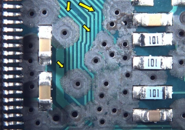
Common Copper Plating Defects
Typically, the following defects can occur with copper plating
Void Formation
Void defects are complete or partial missing copper areas inside plated holes. They cause open circuits or high-resistance connections.
These voids are caused due to:
- Poor desmear leading to non-conductive spots.
- Air entrapment during plating.
- Incomplete wetting of hole walls.
To prevent these issues, it is important to:
- Optimize pre-cleaning, desmear, and pre-dip chemistry.
- Use ultrasonic agitation or air sparging.
- Maintain balanced bath additives to prevent gas pittin
Barrel Cracking
Barrel cracks appear after solder reflow or thermal cycling as circumferential fractures along the plated wall.
Typically, root causes for barrel cracking include:
- High internal stress in the copper deposit.
- Over-etching or a thin electroless seed layer.
- CTE (Coefficient of Thermal Expansion) mismatch between copper and resin.
Here is hw to tackle barrel cracking:
- Control additive levels for low-stress deposits.
- Avoid aggressive pre-treatments.
- Verify plating thickness uniformity.
Nodule and Dendrite Growth
Nodules are localized protrusions; dendrites are needle-like copper formations. Both compromise insulation resistance and may trigger shorts in fine-pitch boards.
Nodules are caused by:
- Excessive organic additives or contamination.
- Localized current density spikes.
- Poor anode bag filtration.
To mitigate these issues:
- Regularly filter the bath and clean the anode bags.
- Optimize agitation.
- Maintain stable chloride ion levels (~30 ppm)
Source: https://www.pcbdirectory.com/community/causes-of-pcb-corrosion-and-how-to-prevent-it
Burnt Deposits
Burnt or rough deposits occur near high-current-density regions, such as hole entries or board edges.
Burnt deposits are caused by:
- Overvoltage or poor current distribution.
- Depleted brighteners or suppressors.
- Insufficient agitation.
To avoid burnt deposits, designers must ensure:
- Reduce current density gradually during startup (ramp plating).
- Refresh the additive ratio.
- Inspect rectifier ripple (<5%).
Pitting
Burnt deposits are caused by:
- Entrapped gas bubbles.
- Particulate contamination.
- Organic decomposition products.
To avoid pitting:
- Maintain clean filters (≤5 μm).
- Avoid over-agitation.
- Replace aging bath regularly.
Recommended Reading: PCB Copper Pouring: Why Filling Empty Areas is Critical for Manufacturing
Analytical Control and Bath Maintenance
Regular Monitoring Parameters
A stable plating bath requires chemical analysis and control of replenishment. Critical parameters include:
| Parameter | Recommended Frequency | Measurement Method |
|---|---|---|
| Cu²⁺ concentration | Daily | Titration |
| H₂SO₄ concentration | Daily | Acid-base titration |
| Cl⁻ ion level | Daily | Argentometric |
| Additive concentration | Twice per shift | CVS (Cyclic Voltammetric Stripping) |
Automatic dosing systems often use CVS readings to maintain additive levels within ±10% tolerance.
Filtration and Agitation
Fine filtration (5 µm polypropylene cartridges) prevents particle buildup that causes pitting or nodules. Agitation via air sparging or eductor jets maintains homogeneity but must be controlled to avoid air bubble entrapment in deep vias.
Temperature and pH Stability
Although acid copper baths operate near pH ≈ 0.5, local pH increases can occur at the cathode. Proper mixing prevents precipitation of Cu(OH)₂ and additive degradation.
Temperature deviations greater than 5 °C impact throwing power, leading to thin hole-center plating.
Emerging Technologies in Copper Plating
Copper plating in the modern age has gone through various technological innovations. Here are a few emerging concepts worth discussing.
Pulse and Pulse Reverse Electroplatin
Instead of continuous DC, pulse plating periodically switches current on and off, enhancing ion diffusion. Pulse reverse plating (PR) extends this by applying short reverse currents to dissolve protrusions selectively.
Pulse reverse plating helps in enhancing plating efficiency by providing:
- Uniform thickness in high-aspect-ratio vias (AR > 12:1).
- Reduced internal stress and improved ductility.
Additive-Free or Low-Additive Baths
Recent research promotes simplified bath formulations using surfactant-stabilized dispersions or ionic liquids to minimize the environmental impact of organic additives.
While not yet standard in large-scale production, they promise greater stability and recyclability.
Direct Metallization Alternatives
Some manufacturers now replace the palladium-catalyzed electroless process with carbon-based or graphite-based direct metallization, reducing cost and waste.
These techniques eliminate formaldehyde, meeting increasingly strict environmental regulations (e.g., RoHS, REACH).
Conclusion
The chemistry of copper plating in PCB production is both a science and an art. Precise control of bath composition, additives, current density, and agitation ensures the essential balance between throwing power, grain structure, and stress control.
When properly managed, copper plating produces durable interconnects that withstand multiple thermal cycles and assembly operations — extending the life of the entire electronic system.
Frequently Asked Questions
1. What determines the uniformity of copper plating in PCB holes?
Uniformity is influenced by current density distribution, agitation, plating bath chemistry, and additive balance. Pulse plating methods further improve uniformity in deep vias.
2. Why are additives necessary in copper plating baths?
Additives (suppressors, accelerators, and levelers) regulate deposition rate and surface morphology, helping achieve bright, ductile, and uniform copper layers.
3. How do barrel cracks form, and how can they be prevented?
Barrel cracks arise from internal stress or inadequate copper thickness in the hole walls. They are prevented by maintaining correct additive ratios, deposition stress control, and sufficient plating thickness.
4. What’s the role of chloride ions in the plating bath?
Chloride ions stabilize the interaction between suppressors and accelerators, improving deposit smoothness. Concentrations should stay around 30–50 mg/L.
5. How often should plating chemistry be analyzed?
Key bath parameters (Cu²⁺, acid, chloride, and additives) should be analyzed daily, with additive levels checked at least twice per production shift for consistent plating quality
References
- Z. Peterson, “Direct metallization process for PCB via fabrication,” Altium Resources, Jun. 13, 2024. [Online]. Available: https://resources.altium.com/p/direct-metallization-process-pcb-fabrication
- M. C. López, “Plated through via (PTV) manufacturing defects,” doEEEt.com, Mar. 13, 2020. [Online]. Available: https://www.doeeet.com/content/testing-eee-parts/plated-through-via-ptv-manufacturing-defects/
- “Optimization of through-hole plating method for prototyping,” Academia.edu, 2015. [Online]. Available: https://www.academia.edu/126413501/Optimization_of_through_hole_plating_method_for_prototyping
- “Effect of chemical and processing parameters on hole filling,” Electronics.org. [Online]. Available: https://www.electronics.org/system/files/technical_resource/E5&S19_01.pdf
- “Summary of PCB electroplating process knowledge,” KingfordPCB.com, Oct. 31, 2022. [Online]. Available: https://www.kingfordpcb.com/engineering-technology/1352.html
- “Via fill and through hole plating process with enhanced TH,” Electronics.org. [Online]. Available: https://www.electronics.org/system/files/technical_resource/E41&S01_03%20-%20Maria%20Nikolova.pdf


