
One of the most critical and foundational decisions in electronic design is selecting the right printed circuit board (PCB) layer stack-up. This choice forms the very backbone of your product, directly impacting its performance, reliability, size, and cost. Choosing a circuit board that’s too simple can lead to signal integrity issues and functional failure. Conversely, opting for an overly complex board can needlessly inflate your budget and timeline.
This guide is designed to cut through the confusion. We will provide a clear, detailed comparison of single-sided, double-sided, and multi-layer PCBs, equipping you with the knowledge to make the most informed and cost-effective decision for your next project.
What Are Single-Sided, Double-Sided, and Multi-Layer PCBs?
Before diving into the comparison, let’s quickly define the three main types:
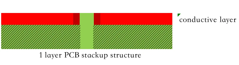
Single-Sided PCBs:
These are the simplest and most fundamental type of PCB. They have a single layer of conductive copper laminated on one side of a non-conductive substrate (like FR-4). All components are placed on one side, and all traces are routed on the other.
- Alt: Diagram of a single-sided PCB showing components on top and copper traces on the bottom.
Double-Sided PCBs:
These boards have conductive copper layers on both sides of the substrate. Plated through-holes (PTHs) or vias are used to create electrical connections between the top and bottom layers, allowing for much more complex and dense routing.
- Alt: Cross-section of a double-sided PCB illustrating plated through-holes connecting the top and bottom copper layers.

Multi-Layer PCBs:
These consist of three or more layers of conductive copper, separated by insulating layers and laminated together into a single structure. They can range from 4 layers to over 50 in advanced applications. Internal layers are connected using vias, which can be through-hole, blind, or buried.
- *Alt: Detailed stack-up of an 8-layer multi-layer PCB, showing internal power and signal planes along with microvias.*

The Great Trade-Off: A Detailed Comparison
Feature
Single-Sided PCB
Double-Sided PCB
Multi-Layer PCB (4-Layer Example)
Cost
Lowest
Moderate
Highest
Design Complexity
Very Low
Medium
MediumHigh to Very High
Circuit Density
Low
Medium
High
Signal Integrity
Poor (risk of crosstalk)
Good (with careful layout)
Excellent (dedicated planes)
Power & Noise
Limited power handling, noisy
Better, but no dedicated plane
Excellent, with stable power & low EMI
Size & Weight
Larger, heavier for function
Smaller than single-layer
Smallest and lightest
Reliability
Good for simple applications
Good
Highest (robust construction)
Typical Applications
Calculators, toys, simple switches
Power supplies, LED strips, auto dashboards
Smartphones, routers, medical devices
Single-Sided PCBs: The Low-Cost Champion
Advantages:
- Extremely Low Cost: The simple manufacturing process makes them the most affordable option by far, ideal for high-volume, cost-sensitive products.
- Simple Design and Fabrication: The simple manufacturing process makes them the most affordable option by far, ideal for high-volume, cost-sensitive products.
- Ease of Repair: The simple manufacturing process makes them the most affordable option by far, ideal for high-volume, cost-sensitive products.
Disadvantages:
- Low Circuit Density: Limited to one routing layer severely restricts the complexity of the circuits that can be implemented.
- LPoor Signal Integrity: The lack of a ground plane makes the board susceptible to noise, crosstalk, and EMI, unsuitable for high-speed or sensitive analog circuits.
- Large Physical Size: Complex circuits require a much larger board area compared to double or multi-layer alternatives.
When to Choose Single-Sided:
Choose a single-sided PCB if your project is defined by extreme cost sensitivity and simple functionality. It’s perfect for:
- Consumer toys
- Basic electronic calculators
- Simple power relays and switches
- Low-frequency analog circuits
Double-Sided PCBs: The Versatile Workhorse
Advantages:
- Increased Circuit Density: By utilizing both sides of the board and connecting them with vias, you can route more complex circuits in a smaller area.
- Improved Design Flexibility: Designers can cross traces on different layers, simplifying the overall routing process.
- strong>Cost-Effective for Mid-Range Projects: They offer a excellent balance of enhanced capability and reasonable cost, avoiding the premium of multi-layer boards.
Disadvantages:
- Higher Cost than Single-Sided: The addition of a second copper layer and the plating process for vias increases the cost.
- More Complex Design: Requires careful planning of via placement and layer transitions.
- Limited Performance for Advanced Applications: While better than single-sided, they still lack the inherent noise shielding and dedicated power planes of multi-layer boards.
When to Choose Double-Sided:
A double-sided PCB is the ideal all-rounder. It’s the most common choice for a vast range of applications, including:
- Power supplies and converters
- Automotive dashboards and lighting
- Industrial control systems
- Consumer audio equipment
- Prototyping and development boards
Multi-Layer PCBs: The High-Performance Powerhouse
Advantages:
- Superior Signal Integrity and EMC: Dedicated internal ground and power planes provide excellent shielding, reduce cross-talk, and ensure stable impedance for high-speed signals.
- High Circuit Density in a Small Form Factor: By stacking multiple layers, incredibly complex circuits can be packed into a very small space, essential for modern compact devices.
- Enhanced Reliability: The laminated structure is robust and better suited for harsh environments with thermal and mechanical stresses.
- Reduced EMI Emissions: The shielding effect of internal planes contains electromagnetic interference, helping products meet strict EMC regulations.
Disadvantages:
- Highest Cost: The complex manufacturing process involving lamination and precision drilling significantly increases the price.
- Complex Design and Fabrication: Requires advanced EDA tools and experienced designers. The fabrication process is longer and has a higher potential for yield loss.
- Challenging Debugging and Rework: Diagnosing and repairing faults on internal layers is extremely difficult, if not impossible.
When to Choose Multi-Layer:
Choose a multi-layer PCB when performance, size, and reliability are non-negotiable. They are essential for:
- Smartphones, laptops, and tablets
- High-speed digital designs (processors, FPGAs)
- Medical imaging and diagnostic equipment
- Aerospace and defense systems
- RF and wireless communication devices (4G/5G routers)
Key Factors to Guide Your Choice
To make the final decision, systematically evaluate your project against these criteria:
Circuit Complexity and Size:
How many components and connections are there? Can they be routed on one or two layers without becoming excessively large?
Signal Speed and Integrity:
Are you dealing with high-frequency digital signals (e.g., DDR memory, Gigabit Ethernet) or sensitive analog signals (e.g., sensors, audio amplifiers)? If yes, a multi-layer board with dedicated planes is almost mandatory.
EMI/EMC Requirements:
Does your product need to pass stringent electromagnetic compatibility certifications? Multi-layer boards provide inherent shielding that is hard to achieve otherwise.
Power Requirements:
Does your design have multiple voltage levels and require stable, low-noise power delivery? Internal power planes in a multi-layer PCB are the best solution.
Budget and Timeline:
Be realistic. A single or double-layer board will always be cheaper and faster to produce than a multi-layer one. Does your performance requirement justify the extra cost and time?
Conclusion: Making an Informed Decision is Key
There is no one-size-fits-all answer in PCB design. The right choice is the one that optimally aligns with your project’s specific technical demands and commercial constraints.
- Choose Single-Sided for simple, low-cost, high-volume products.
- Choose Double-Sided for the vast majority of versatile, mid-complexity electronic devices.
- Choose Multi-Layer for high-speed, high-density, and high-reliability applications where performance is paramount.
Still unsure which PCB stack-up is the perfect foundation for your next big idea? Don’t leave it to chance. The experts at WWELLER are here to help. Contact us today for a free design review and quotation. We’ll analyze your requirements and recommend the most optimal and cost-effective PCB solution to ensure your project’s success.


