
Optimizing PCB Design for a Seamless Assembly Process
A smooth PCB assembly process relies heavily on the initial PCB design data and fabrication specifications. High-quality PCB design not only streamlines subsequent circuit board assembly—enhancing production efficiency and reducing defect rates—but also safeguards the quality of the final assembled product. Conversely, incomplete or suboptimal designs can disrupt manufacturing workflows and compromise product integrity.

So, what key factors in PCB design significantly influence circuit board assembly? Here are some common issues that PCB designers must pay close attention to.
1. Ensure that silkscreen legends do not overlap with SMD pads or through-hole solder areas.
A common PCB design error is silkscreen over an SMD pad, which interferes with soldering and negatively impacts overall assembly quality and yield.

To balance the need for assembly inspection and soldering quality, a silkscreen outline can be added for critical components. This mark must be clearly offset from the pads, typically at the component corners, to avoid overlapping the SMT soldering zone.

2. The minimum spacing between copper zone and board edge
Critical PCB layout spacings relative to the board edge must be maintained for reliable manufacturing. The standard requirements are: a 0.5mm clearance for any copper, a 4.0mm clearance for solder pads, and a 5.0mm distance for component bodies.
| Design Element | Minimum Distance from Board Edge |
|---|---|
Copper (Traces/Pours) | 0.5 mm |
Solder Pad | 4.0 mm |
Component | 5.0 mm |
3. The Critical Role of Fiducial Marks and Tooling Holes in PCB Assembly Accuracy
In PCB panelization, Fiducial Marks and Tooling Holes play distinct but complementary roles in ensuring precision and efficiency.

Fiducial Marks: The “Eyes” of Assembly Machines:
These high-contrast marks provide a visual reference for automated assembly, guiding machinery to accurately place components. They are critical for achieving soldering precision and are defined by a 1.5mm diameter and a 3.0mm solder mask clearance.
Tooling Holes: The “Anchor Points” for Fabrication:
These non-plated holes (typically 3x 3.0mm) act as fixed anchor points, securing the panel during various processes like electrical testing and profile routing. This prevents shifting and guarantees manufacturing accuracy.
Incorporating fiducial marks and tooling holes correctly is fundamental to a smooth manufacturing workflow. Adhere to the following specifications for optimal results:
Feature | Purpose | Key Specifications |
|---|---|---|
Fiducial Mark | Optical reference for paste printing and component placement. | - Shape: Circular |
Tooling Hole | Mechanical fixation for testing and routing processes. | - Type: Non-plated (NPTH) |
4. Metal-shell components layout notes
When designing double-sided PCBs, special attention must be paid to metal-shell components. In DIP (Dual In-line Package) applications where the component housing contacts the printed board, the top-layer solder pads must not remain exposed. Instead, they should be insulated with either solder mask ink or silkscreen ink.
5. Avoid jumper wires
To prevent short circuits and potential electrical failure, never place jumper wires under ICs, motors, potentiometers, or other large metal-shell components.
6. Electrolytic capacitors layout notes
Electrolytic capacitors must maintain a safe distance from heat sources. They are prohibited from contacting high-power resistors, thermistors, transformers, or heat sinks. The required minimum clearance from a heat sink is 10 mm, whereas other standard components require only a 2.0 mm gap.
7. Large or heavy components
Pads for large or heavy components (e.g., transformers, electrolytic capacitors >15mm, high-current connectors) must be reinforced. This is critical for withstanding mechanical stress during assembly and operation, as well as ensuring sufficient current-carrying capacity.
8. Minimum trace width and spacing
A minimum trace width and spacing of 0.1mm/0.1mm is recommended for most designs. Going below this standard will challenge fabrication capabilities and increase manufacturing costs.
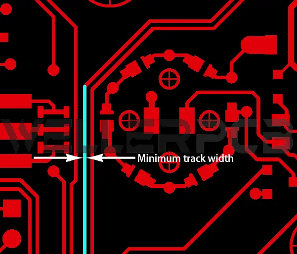

However, for high-density interconnect (HDI) designs with strict physical size constraints, employing finer traces and spaces becomes necessary. In these cases, the performance benefit must be balanced against the higher cost, which remains a critical factor in the decision-making process.
9. Critical Keep-out Area Around Screw Holes
A keep-out area with a 5.0mm radius from any screw hole must be clear of copper planes (unless required for grounding) and components (unless specified in the structural diagram).
10. Through-Hole Pad Size Design Rule
The pad diameter for a standard component mounting hole should be twice the drill hole size. For design feasibility, the minimum recommended pad diameter is 1.5mm for double-sided boards and 2.0mm for single-sided boards. If a circular pad is not suitable, an oval (waist) pad is an acceptable alternative.
Follow these rules for robust through-hole (PTH) connections:
- Pad-to-Hole Ratio: Pad Diameter ≈ 2 x Finished Hole Diameter
- Minimum Pad Diameter:
- PDouble-Sided Boards: 1.5 mm
- Single-Sided Boards: 2.0 mm
- Pad Shape: Circular pads are standard; oval (waist) pads are permitted where space is constrained.
11. Implement Silkscreen Separation
For pads with a center-to-center spacing of less than 2.5mm, a 0.2mm silkscreen outline must be applied between them. This practice is critical to prevent solder bridging during assembly and ensure electrical isolation.
12. Preventing Solder Steal in Wave Soldering
For any design utilizing wave soldering, proactively design solder pads to counteract the solder flow. By offsetting the pad (0.5mm – 1.0mm) in the direction opposite to the wave, you effectively prevent solder theft from the secondary side pads, eliminating a common source of manufacturing defects and ensuring robust solder joints.Follow this guideline:
- Orientation: Design the solder pad to open in the direction opposite to the board’s travel through the wave.
- Offset: Position the pad with a 0.5mm to 1.0mm offset from the lead. This ensures sufficient solder fillet formation and prevents poor joints caused by solder being drawn away from the pad.
13. Warpage Prevention for Large Panels
PCB designs exceeding 500 cm² must include a dedicated component-free strip, 5mm to 10mm wide, running through the panel center. This zone is reserved for installing stiffening bars to prevent board bending and warpage during wave soldering.Follow this guideline:
- Reserve a Central Channel: Maintain a clear, component-free zone (5mm to 10mm wide) along the panel’s center.
- Purpose: This channel is used to attach stiffening bars (bending bars), which reinforce the panel structurally as it passes through the high-temperature solder wave, preventing bending.
14. Apply Solder Mask Tenting to All Vias
All plated through-hole vias must be designed as “tented vias”—completely covered by solder mask without openings. This practice is critical for preventing solder from flowing into the via holes during soldering, which is a common cause of solder shorts and insufficient joint formation on component pins.
15. Ensure Proper Component Spacing
Components must maintain sufficient physical spacing to prevent tombstoning and solder bridging. Inadequate clearance between SMD or through-hole components is a primary cause of placement and soldering defects, disrupting the assembly process.
Optimize Your Design for Flawless Assembly
These are some of the most common PCB layout considerations that directly influence assembly success. For designers, adhering to these principles is key to avoiding costly re-spins and production delays.
Contact Us Today
For further engineering support, email our experts at [email protected]. We look forward to helping you with your project and will get back to you within one business day.


