Table of Contents

HDI PCB Design, Manufacturing, Assembly, and Sourcing Guide

An HDI PCB is a high-density interconnect printed circuit board. It uses finer traces, smaller vias, and denser routing than a standard board. Most designs use microvias, blind vias, buried vias, or via-in-pad structures to connect more signals in less space.
Use HDI when a standard multilayer board cannot support your component density, BGA fanout, product size, or signal performance goals. HDI can improve routing and reduce board size, but it also adds fabrication cost, lead time, and reliability checks.

What Is an HDI PCB Board

An HDI board has higher wiring density per unit area than a conventional printed circuit board. In practical terms, it can route more connections through a smaller board area while supporting compact components and tighter layouts.

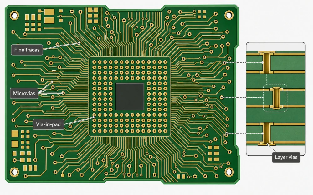
HDI technology often includes microvias, blind vias, buried vias, via-in-pad, fine trace and space, thin dielectric layers, dense component placement, sequential lamination, and controlled impedance routing.

Core Via Structures

Core Via Structures

A microvia is a small via usually used to connect adjacent layers. A blind via connects an outer layer to an inner layer. A buried via connects internal layers only. Via-in-pad places a via inside a component pad, often for fine-pitch BGA routing.

For formal HDI design terminology and microvia guidance, engineers often refer to the IPC-2226 HDI printed board design standard.

Common B2B Applications

  • Medical electronics and compact diagnostic devices
  • Automotive ADAS modules and control electronics
  • IoT devices, wireless modules, and wearables
  • 5G, telecom, and high-speed digital products
  • Industrial control boards and compact embedded systems

WellerPCB works with PCB fabrication, PCB assembly, and electronics manufacturing projects where early design review can help reduce avoidable production risk.

HDI PCB vs Standard PCB: Key Differences

HDI vs Standard PCB Key Differences
A standard multilayer PCB can work well for many products. However, HDI becomes useful when through-hole vias and standard design rules consume too much routing space or block critical signal paths.
Feature Standard PCB HDI PCB Design or Manufacturing Impact
Main via type Through-hole vias Microvias, blind vias, buried vias, via-in-pad Frees routing space but needs tighter process control
Routing density Moderate High Better for fine-pitch components and dense layouts
Stackup complexity Lower Higher Requires earlier stackup planning
Manufacturing process Standard lamination and drilling Sequential lamination, laser drilling, via filling Can increase cost and schedule risk
Assembly impact Usually simpler Often fine-pitch SMT or BGA May need closer DFA review and inspection planning

When Standard Construction May Be Enough

A standard PCB may be enough if the layout has enough routing area, the components have relaxed pitch, and through-hole vias do not block critical channels. Therefore, teams should not choose HDI only because it sounds more advanced.
For designs between conventional multilayer construction and HDI, a multilayer PCB stackup review can help confirm the right direction.

When Should You Use HDI PCB Technology

Fine-Pitch BGA
Use HDI only when it solves a defined engineering problem. It is not the best default choice for every multilayer board, especially when cost, schedule, or fabrication simplicity matters more than density.

Fine-Pitch BGA or High-I/O Components

Fine-pitch BGA packages often drive HDI decisions. If you cannot escape inner rows with standard dogbone fanout and through-hole vias, microvias or via-in-pad may be needed. For dense packages, a fine-pitch BGA PCB design review can prevent routing and assembly problems later.

Compact Form Factor or Layer Count Pressure

HDI can reduce board area by allowing tighter routing. In some designs, it may also help avoid adding too many conventional layers. This is not automatic. A poor stackup can raise cost without solving the layout problem.

High-Speed or Impedance-Controlled Designs

HDI can shorten interconnects and reduce via stubs. It can also support controlled impedance with thinner dielectrics and tighter stackup control. If impedance is a major requirement, validate the structure with PCB impedance calculation and fabricator feedback.

HDI PCB Design Checks Before Layout Release

HDI design works best when the fabricator is involved before layout is locked.
Stackup, via type, trace width, materials, surface finish, solder mask, and assembly access all affect cost and yield.

Stackup Planning

HDI stackups often use terms such as 1+N+1, 2+N+2, or 3+N+3. The N is the core multilayer section. The numbers show how many build-up layers are added on each side. More build-up layers increase routing options, but they also increase lamination cycles and process risk.

Via Choices and Risk Checks

Via structure affects routing density, lamination steps, inspection needs, and long-term reliability. Therefore, each HDI via choice should be checked before the layout is released.

Design Choice Why It Is Used Manufacturing Impact Risk To Check
Blind via Connects an outer layer to an inner layer Requires controlled drilling or laser processing Registration and plating quality
Buried via Connects internal layers only Adds internal processing steps Lamination complexity
Microvia Supports dense adjacent-layer routing Often laser drilled Aspect ratio and reliability
Stacked microvia Saves space in vertical transitions Needs more complex filling and plating Thermal fatigue and cracking
Via-in-pad Helps fine-pitch BGA fanout Needs filling, plating, and planarization Solder defects if poorly processed

For BGA-heavy designs, review the manufacturing impact of via-in-pad technology before routing is complete.

Rules, Materials, and Surface Finish

Do not design to generic internet numbers. Use your supplier’s current capability for trace width, spacing, microvia size, drill-to-copper clearance, annular ring, capture pad, solder mask clearance, copper weight, board thickness, and impedance tolerance.
Material choice matters more when the stackup is thin, dense, or high-speed. Relevant properties include Tg, CTE, dielectric thickness, Dk, and Df. A PCB base material selection review is useful when the design has thermal, impedance, or reliability requirements.
Fine-pitch SMT and BGA assembly often need a flat surface finish. Compare PCB surface finish options before release if solderability, shelf life, or assembly yield is a concern.

DFM and DFA Package Before Release

  • Gerber, ODB++, or IPC-2581 fabrication data
  • Drill files, stackup drawing, and panelization requirements when applicable
  • Controlled impedance, material, copper weight, and surface finish requirements
  • Solder mask, silkscreen, polarity marks, and assembly notes
  • BOM, Pick and Place files, and assembly drawings if PCBA is included
  • Testing, inspection, or functional test requirements
A DFM review should happen before purchase order release, not after the design is already late. WellerPCB can support project teams with DFM issue checks before PCB manufacturing when the design package is ready for review.
If your team is preparing an HDI design for prototype or production review, share the stackup goal, fabrication files, impedance notes, BOM, Pick and Place files, assembly drawings, and test expectations early. A short technical review before release can be more useful than fixing avoidable issues after fabrication starts.

How HDI PCB Boards Are Manufactured

HDI manufacturing uses many standard PCB steps, but adds tighter process control and extra build-up work. The design should match the process before fabrication starts.

Sequential Lamination and Build-Up Layers

Sequential lamination builds layers in stages. The manufacturer processes the core, adds dielectric and copper layers, forms vias, plates them, and repeats the process as needed. More lamination cycles usually mean more cost, longer lead time, and more chances for registration or reliability issues.

Laser Drilling, Filling, and Plating

Microvias are commonly formed with laser drilling. After drilling, vias are cleaned, metallized, plated, and sometimes filled. Via-in-pad structures need extra care because solder can wick into poorly filled vias during assembly.

Common Fabrication Risks

  • Layer registration errors
  • Laser drill variation
  • Via plating or filling defects
  • Fine-line etching variation
  • Solder mask alignment issues
  • Warpage or impedance mismatch
For advanced builds, route the project through an HDI PCB manufacturing capability review instead of treating it like a standard rigid board order.

HDI PCB Assembly, Testing, and Reliability

HDI is often used with dense SMT assembly, fine-pitch BGA packages, and compact product layouts. Therefore, fabrication and assembly should not be treated as separate decisions.

Layout choices affect soldering, inspection access, test coverage, repair difficulty, and long-term reliability. This is why HDI projects need both DFM and DFA review before production release.

Fine-Pitch SMT and Mixed Assembly Risks

Fine-pitch BGA assembly needs flat pads, clean solder mask definition, controlled paste volume, and proper reflow profiling. In addition, mixed SMT and through-hole designs need enough spacing for placement, soldering, inspection, and repair access.

If the same supplier handles fabrication and PCB assembly, DFM and DFA feedback can be combined before the design reaches production.

Inspection and Test Options

Method What It Helps Check Where It Fits
Visual inspection Surface defects, markings, polarity, and workmanship issues Fabrication and assembly
AOI Solder mask, component placement, and visible solder joints Fabrication and assembly
X-ray inspection Hidden BGA solder joints and via-in-pad issues PCBA
Electrical or flying probe test Opens, shorts, and prototype electrical checks Bare board or assembly
ICT Node-level checks when fixture access and volume justify it Production PCBA
Impedance test Controlled impedance trace validation Bare board
Functional testing Product-level operation Final PCBA

Not every project needs every test. However, dense HDI boards usually need more inspection planning than simple rigid PCBs.

For assembled boards, AOI inspection and functional testing can support quality validation when they match the product requirements.

Common Reliability Risks

Common HDI reliability issues include microvia cracking, delamination, voided vias, poor plating, solder voids, BGA defects, and impedance mismatch.

Many of these risks start in design. As a result, a manufacturable stackup, realistic via structure, compatible material choice, and clear documentation can reduce problems before fabrication begins.

For additional background on HDI quality and acceptability concerns, see Altium’s overview of HDI quality requirements.

Cost, Lead Time, and Supplier Selection

HDI cost is driven by complexity. The main drivers are layer count, lamination cycles, microvia structure, material choice, via filling, surface finish, inspection, order quantity, and the amount of engineering review needed before release.

Questions To Ask a Supplier

  1. What stackup options can you review for this design?
  2. Can you assess the required microvia and via-in-pad structure?
  3. Can you review controlled impedance before fabrication?
  4. Which materials and surface finishes are compatible with the design?
  5. What inspection and test options fit the project risk?
  6. Can the supplier support prototype and production handoff?
  7. What files are needed for DFM and DFA review?

Prototype-to-Production Risk

A design may pass an early prototype build but still need changes before stable production. If the project may scale, consider the handoff needs described in prototype-to-mass-production PCB practices.

Documentation for Quote and Review

Prepare fabrication files, stackup requirements, drill table, impedance data, material notes, surface finish requirements, BOM, Pick and Place file, assembly drawing, and test plan when possible. Missing data can delay quotation, DFM review, fabrication, and assembly.

HDI is worth using when it solves a real density, size, BGA fanout, or signal performance problem. The strongest projects align layout, stackup, fabrication, assembly, testing, and supplier review before the design is released.

FAQs

What does HDI PCB mean?
HDI PCB means high-density interconnect printed circuit board. It uses smaller vias, finer traces, and tighter routing than standard PCB construction. Engineers use it when dense components, compact size, or high-speed routing cannot be handled well with conventional vias.
A standard multilayer PCB can have many layers, but it often relies on through-hole vias. HDI uses microvias, blind vias, buried vias, and sometimes via-in-pad to increase routing density and support fine-pitch components in less space.
Choose HDI when a clear design constraint requires it, such as fine-pitch BGA fanout, limited board area, high I/O density, or controlled high-speed routing. If normal vias and standard stackup rules work, standard fabrication may be simpler.
HDI manufacturing may require sequential lamination, laser-drilled microvias, via filling, tighter registration, fine-line etching, and added inspection. Each extra build-up layer or advanced via structure can increase process complexity, so early DFM review is recommended.
HDI often appears with fine-pitch SMT and BGA components. Assembly may require flatter pads, controlled solder paste, good reflow profiling, and X-ray inspection for hidden joints. DFA review should check via-in-pad, stencil, spacing, polarity, and test access.
By 凯文

I have over 10 years of experience in PCB manufacturing. My work includes PCB fabrication, SMT assembly, DFM review, supplier communication, and electronics production support. In my writing, I explain PCB design, layer stack-up, assembly processes, quality control, and production planning in a practical way. My goal is to help readers make better manufacturing decisions.

Recent Posts

Get In Touch With Us Today

Drag & Drop Files Here (dsn, pdf, xlsx, dxf, zip, rar up to 8M)
or
This form is protected by Google’s Terms of Service and Privacy Policy.

Related Posts

FPGA vs Microcontroller for PCB Design and Assembly

Choose a microcontroller when a product needs simple control, low power, lower cost,.

VCC vs VDD vs VSS

VCC and VDD usually mean the positive power rail. VSS usually means the.

Leave a Reply

Your email address will not be published. Required fields are marked *