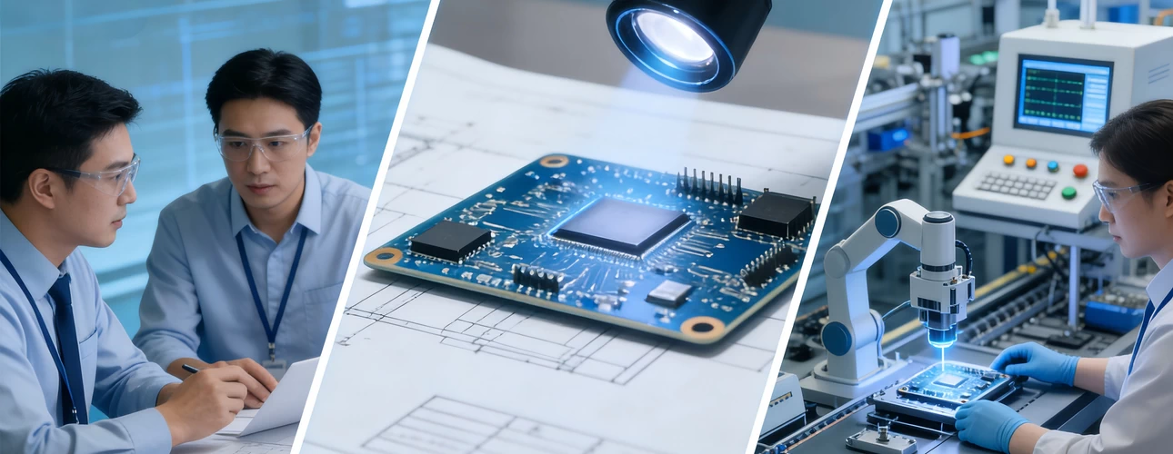
In the electronics industry, building a working prototype is only the first step. The real challenge begins when that prototype must be converted into a reliable, cost-effective product that can be manufactured in large volumes. This transition is known as New Product Introduction (NPI), and it plays a critical role in the success of any electronic hardware product.
For companies involved in PCB design, PCB manufacturing, and electronics assembly, a well-executed NPI process ensures smooth scaling from prototype to mass production. This article explains the best practices for NPI for PCB design for engineers and PCB designers.
What is NPI and Why it’s Critical in PCB Manufacturing
New Product Introduction (NPI) is the structured process that prepares a new electronic product for manufacturing. In PCB design and electronics manufacturing, NPI ensures that the circuit board can be produced repeatedly with consistent quality, performance, and yield.
A prototype PCB is usually built to validate functionality. Engineers may hand-solder components, use development boards, or select parts based on short-term availability. However, mass production requires stable designs, controlled components, automated assembly, and reliable testing.
The difference between these two stages is often underestimated.
Aspect | Prototype PCB | Production PCB |
|---|---|---|
Quantity | 1–10 boards | Thousands of boards |
Assembly | Manual soldering | Automated SMT lines |
Components | Flexible selection | Approved and locked |
Testing | Production-grade testing | Basic functional tests |
For example, a prototype IoT controller board may work perfectly in the lab, but during production, the same board may fail due to solder bridging, component shortages, or thermal issues. NPI exists to prevent such surprises.
Suggested Reading: PCB Design Optimization for Compact and Connected IoT Devices
PCB Design for Manufacturability and Assembly
A smooth NPI process begins at the PCB design stage. If a board is not designed for manufacturing and assembly, problems will arise later, when fixes become expensive and time-consuming.
Design for Manufacturability (DFM) ensures the PCB can be fabricated reliably. This includes proper trace widths, spacing rules, via sizes, stackup selection, and solder mask design. Ignoring these aspects may result in low yields or fabrication delays.
Design for Assembly (DFA) focuses on the placement and soldering of components. In production environments, automated pick-and-place machines require consistent component orientation, sufficient spacing, and standard footprints.
As an example, placing multiple resistor networks with random orientations may not affect prototype performance, but it significantly increases assembly errors during high-volume SMT production. Similarly, placing connectors too close to the PCB edge may cause mechanical failures in the field.
Involving PCB manufacturers and assembly partners early in the design phase allows engineers to address DFM and DFA issues before they become production bottlenecks.
Suggested Reading: Top 10 DFM Issues that Affecting PCB Manufacturing
BOM Optimization and Supply Chain Readiness
In the PCB and electronics industry, the Bill of Materials (BOM) can make or break a product during NPI. A prototype BOM often focuses on what is available quickly, not what is suitable for long-term production.
During NPI, BOM optimization becomes essential. Every component must be evaluated for lifecycle status, lead time, cost, and availability from multiple suppliers.
BOM Factor | Impact on NPI |
|---|---|
Component life-cycle | Prevents redesigns |
Lead time | Ensures on-time production |
Alternate parts | Reduces supply risk |
Cost stability | Protects profit margins |
For example, selecting a specific voltage regulator IC that later goes end-of-life can force a complete PCB redesign. Similarly, using a microcontroller with a 40-week lead time can delay product launches. A production-ready BOM ensures that scaling from 100 boards to 10,000 boards does not introduce unexpected delays or cost increases.
Prototype Validation, Electronics Testing, and Pilot Builds
Testing is a core part of NPI, especially in electronics and PCB manufacturing. The goal is not just to verify functionality, but to validate performance under real-world conditions.
Prototype testing typically includes functional testing, electrical measurements, thermal analysis, and stress testing. For power electronics or motor control PCBs, thermal testing is especially important to ensure components remain within safe operating limits.
Once prototypes pass validation, pilot production begins. A pilot build uses the same PCB fabrication process, assembly line, and test methods planned for mass production. This stage often reveals issues such as solder defects, incorrect footprints, or test coverage gaps.

For example, a PCB designed for automated optical inspection (AOI) may fail inspection if silkscreen markings overlap pads or component spacing is insufficient. Identifying such issues during pilot production saves significant time and cost later
Suggested Reading: Advanced Uses of PCB Silkscreen in PCB Design
Reliability Engineering and Environmental Testing in NPI
Beyond basic functional checks, modern electronics must withstand real-world operating conditions. Reliability engineering during NPI ensures PCBs perform consistently over time—not just when they are new.
Reliability and environmental testing simulate the stresses a product will experience throughout its lifecycle, making them essential for sectors such as industrial automation, automotive electronics, medical devices, and outdoor IoT systems.
Common reliability tests include:
- Thermal cycling
- Vibration testing
- Humidity exposure
- Extended burn-in testing
For example, a PCB used in a motor drive may pass functional tests but fail after repeated heating and cooling cycles due to solder joint fatigue. Identifying such issues during NPI allows engineers to improve component selection, PCB layout, or thermal design before mass production.

Reliability testing also helps validate design decisions such as copper thickness, PCB material selection, and enclosure design. A high-power PCB may require thicker copper or improved thermal vias to ensure long-term stability. Similarly, boards exposed to moisture may need conformal coating or improved solder mask coverage.
Documentation and Engineering Change Control
Clear documentation is critical to a smooth NPI process. Manufacturing teams depend on accurate, revision-controlled data to build and test PCBs correctly.
Key NPI documents include:
- Fabrication and assembly drawings
- Pick-and-place files
- Test procedures and programming instruction
- Revision history and change logs
All documents must align with the exact PCB revision in production.
Likewise, engineering change control is equally important. Typically, design changes are common during NPI, but unmanaged updates can disrupt manufacturing. Every change should be formally reviewed, documented, and communicated to all stakeholders
Regulatory Compliance, Quality Systems, and Certification Readines
As products approach mass production, regulatory and quality requirements become critical. Many PCBs must meet regional and industry-specific standards before market release. During NPI, compliance planning ensures alignment with:
- EMC and electrical safety standards
- Environmental regulations (RoHS, REACH)
Ignoring compliance early can lead to redesigns or launch delays. For example, poor PCB layout may cause EMC failures late in development. Addressing grounding, shielding, and signal routing during NPI helps prevent this.
Quality systems further support NPI success through:
- Documented inspection and test processes
- Traceability and controlled workflows
These are especially vital in medical, automotive, and other safety-critical industries.
Scaling to Mass Production in the PCB Industry
After successful pilot builds, the product moves into mass production. At this stage, consistency and monitoring become critical. Stable suppliers, repeatable assembly processes, and well-defined quality metrics ensure long-term success. To provide continuous product improvement, the following metrics can be quite helpful:
- First-pass yield
- Defect rates
- Field failure
In the PCB design industry, working with an experienced NPI partner can significantly reduce risk. Such partners provide early design feedback, help optimize layouts for manufacturing, and support supply chain planning. This collaboration often shortens time-to-market while improving product quality.
Suggested Reading: The Key to A First-pass Success in PCB Design
Conclusion
New Product Introduction is a critical phase in electronics and PCB manufacturing that determines whether a product succeeds or struggles. A structured NPI approach connects PCB design, component selection, testing, documentation, and manufacturing into a single, controlled process.
When done correctly, NPI reduces cost, improves quality, and ensures a smooth transition from prototype to mass production. For PCB design companies and electronics manufacturers, mastering NPI is essential for delivering reliable, scalable, and competitive product
Frequently Asked Questions
1. What does NPI mean in PCB design?
In PCB design, NPI refers to the process of preparing a circuit board design for reliable and scalable manufacturing.
2. Why is DFM important during NPI
DFM ensures the PCB can be fabricated with high yield and minimal defects, reducing production risks.
3. How does BOM selection affect mass production
Poor BOM selection can cause shortages, redesigns, and cost increases during high-volume manufacturing.
4. What is the role of pilot production in electronics NPI?
Pilot production validates real manufacturing conditions and identifies issues before mass production begins.
5. How can a PCB design company support NP
By offering DFM/DFA reviews, BOM optimization, testing support, and manufacturing guidance throughout the NPI process.
References
- IWDF Solutions, “Top 10 compliance & regulatory requirements for PCB design for 5G wireless,” IWDF Solutions. [Online]. Available: https://iwdfsolutions.com/top-10-compliance-regulatory-requirements-for-pcb-design-for-5g-wireless/.
- Siemens, “DFM resources for PCB design – Valor NPI,” Siemens EDA. [Online]. Available: https://eda.sw.siemens.com/en-US/eda-cloud-solutions/pcb/valor/valor-npi/resources/.
Nagendra, “Feasibility analysis of manufacturing using rapid prototyping: A review,” (DOI: 10.1016/j.matpr.2021.02.390),” Materials Today: Proceedings, vol. 47, pt. 5, pp. 1286-1290, 2021. [Online]. Available: https://www.sciencedirect.com/science/article/abs/pii/S2214785321008968.
Wevolver, “IPC class system: A technical deep dive into patent classification architecture,” Wevolver, Jan. 26, 2025. [Online]. Available: https://www.wevolver.com/article/ipc-class-system.
Wevolver, “IPC class 2 vs class 3: Understanding the critical differences in electronics manufacturing standards,” Wevolver, Aug. 18, 2024. [Online]. Available: https://www.wevolver.com/article/ipc-class-2-vs-class-3.
Wevolver, “What is AOI (automated optical inspection): A comprehensive guide,” Wevolver, Jun. 11, 2023. [Online]. Available: https://www.wevolver.com/article/automated-optical-inspection.


