PCB DFM issues can derail even the most well-intentioned circuit board design. Design for Manufacturing (DFM) is a critical discipline that ensures your PCB can be produced reliably, cost-effectively, and without delays. Ignoring common PCB DFM issues — such as incorrect pad IPC standards, uneven copper distribution, or via-in-pad placement — often leads to assembly failures, rework, and higher production costs. This article covers the top 10 DFM mistakes to help you avoid them and improve your manufacturing yield.
01: First and foremost PCB DFM issue – Incorrect IPC Pad Standards
One of the most critical PCB DFM issues is ensuring component soldering pads meet IPC standards.
The package size of the solder pads on the printed circuit boards that come into contact with the components are very important, as they determine whether the components can be reliably soldered or not. If the PAD package design meets IPC standards, it can ensure the components accurately soldered on the PAD.
02: Avoiding Tombstone Defects with Uniform Pad Patterns
For the components with package 0402, 0201, or less package sizes, it is very important to make sure the soldering PAD designed at a uniformity method. In this way, it can avoid soldering defects of tombstone (a soldering component has been pulled into a vertical or near-vertical position with only one side soldered to the PCB.
It is typically caused by force imbalances during the reflow soldering process.), which commonly lead to the PCB assembly process failures. Also, to achieve the entire soldering reliability, it is very important to have best consistent soldering uniformity for BGA components. The related testing for verifying this is more complexity and expensive, X-ray inspection is a common way to ensure this reliability.
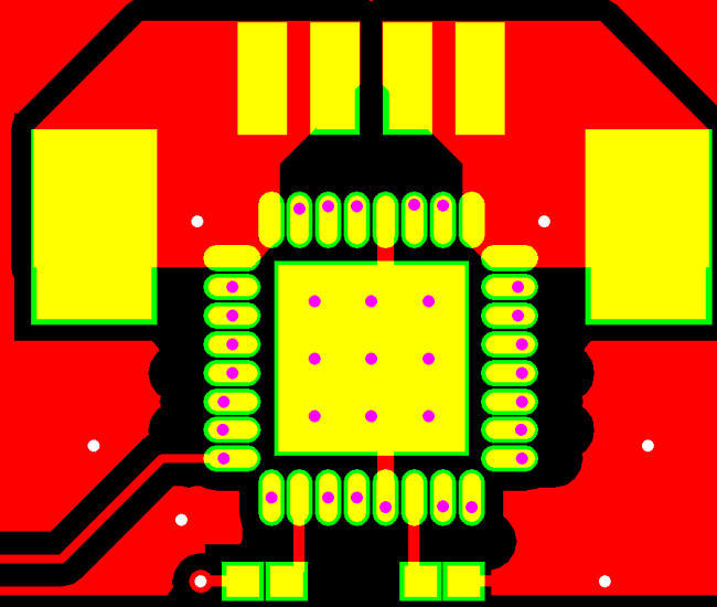
03: The Hidden Risk of Via-in-Pad Placement
It means the via holes placed in the SMD soldering PAD. A basic and common sense in PCB design is that to avoid via holes in PAD as much as possible. The soldering joint would become too weak due to the soldering could leak out through the hole in the PAD. And the electrical circuit may eventually be damaged too. However, in some special field, the design with via hole in PAD is specially used as the solution of thermal heat dissipation.
04: How Uneven Copper Distribution Leads to Board Warpage
Copper pouring on a individual circuit layer is subject to many factors. If there is lack of copper pouring at some specific zones,it may be difficult to maintain a single track transmission performance. Additionally, it maybe take PCB warppage issues if some zones in the circuit layer is lack of basic pouring copper(there will be a bowl and twist after PCB layers lamination process). Therefore, it is recommended to keep the copper distribution as uniform as possible (sometimes the pouring copper is necessary at some signal layers).
No pouring copper
With pouring copper
No pouring copper
With pouring copper
05: Through-Hole vs. Surface Mount – Component Placement Trade-offs
Most PCB designers avoid using through-hole technology (THT) components whenever it is possible, or they directly place all the THT components at same one side of the PCB board.
However, there are cases that the THT components is unavoidable. In these cases, a combination of THT components on the top layer and SMD components on the bottom layer usually allows all components to be placed as close together as possible. However, this situation may not allow the use of single-sided wave soldering, and more expensive methods such as selective wave soldering must be used.
THT-components-PCB-design
SMD-component-PCB-design
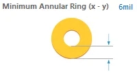
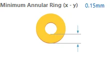
06: Managing Layer-to-Via Offset in Multilayer PCBs
To generate PCB fabrication data is the last process without tolerances in the whole PCB manufacturing chain.
Creation of PCB output data is the final process without tolerance in the manufacturing chain. Tolerances exist in the PCB production process, these tolerances directly reflects from the etching of the copper foil layer and the perforation of the via drilling. Therefore, PCB manufacturers drill the holes after multi-layers stacked togetherly instead of drilling them layer by layer.
It can be imagined that the offset exists between layers and holes, then drilling holes generate the tolerance.Therefore,the design of Minimum Annual Ring and Teardrop can improve the yield of PCB production (Teardrops are used in a PCB layout is to provide extra strength so that the via holes can withstand thermal and mechanical stress.). This indirectly reduces the overall cost of circuit board manufacturing.
07: Should You Remove Non-Connected Via Pads?
Removing non-connected (or no used) vias and pad (the vias, PAD, or PAD of THT components in inner layers) can help PCB manufacturers extend the life of the drill bites. However, some PCB designers do not like this option. From a point of view in electrical performance, removing non-connected (or no used) vias and pad may not affect the final product but probably weaken the physical structure of the product. If you do not want to remove them, it is recommended to specifically remark this requirement in your PCB manufacturing specifications.
08: Minimum Solder Mask Dam Width – 75um Rule
Many PCB designers like to use an practical value of 50um to define the size of solder pads and also define the minimum spacing between solder pads and tracks as 50um. However, if you want a solder dam between two pads, the minimum size should be as 75um. These factors should be considered when creating a component library or placing components on a PCB, otherwise solder mask may not be able to properly cover the zone between solder pads due to too small spacing.
Solder mas dam size in inch
Solder mask dam in mm
09: Optimizing Layer Stackups Before Data Generation
Placing through holes may result in certain copper planes being cut off. However, to avoid this issue, you can slightly make some adjustment as below.
Sharp angles can be restricted through the Altium Design rules:
10: Why Direct SMD Pad Shortcuts Confuse AOI Systems
Direct connections of two SMD pads within or under an SMD component may be acceptable as an electrical shortcut at the time, but they can cause problems during latter testing process. For example, Assembly AOI (Automated Optical Inspection) may not be able to detect the short with a camera, because soldering the connection to the SMD pad would prevent visual inspection. A small change in design can avoid this issue and offer a outstanding convenience to manufacturing process.
Wrong: Direct SMD PAD Connection
Correct: In-direct SMD PAD Connection
From Design to Production: A DFM-First Approach
Designing modern electronic devices is not easy. It requires continuous consideration of electrical, mechanical, and functional aspects throughout the entire development process.
Avoiding these ten common design mistakes is the foundation of a DFM-first PCB development process. From ensuring IPC-compliant pad packages to balancing copper distribution and managing via-in-pad placement, each decision impacts your board’s manufacturability, yield, and long-term reliability. For a structured review, use a DFM checklist for PCB design before finalizing your layout. Contact our engineering team for a free DFM analysis before starting your next high-complexity project.
A graduate of the Electronic Engineering department, with 30+ years of PCB layout experience, focusing on layouts for high-frequency and high-speed circuit boards.