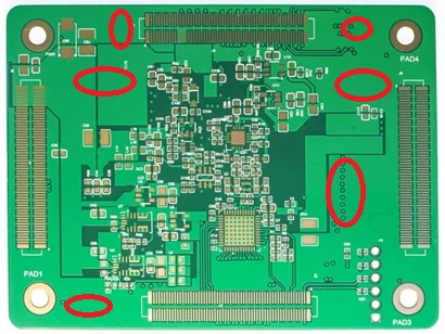
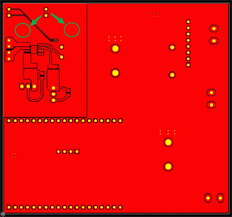
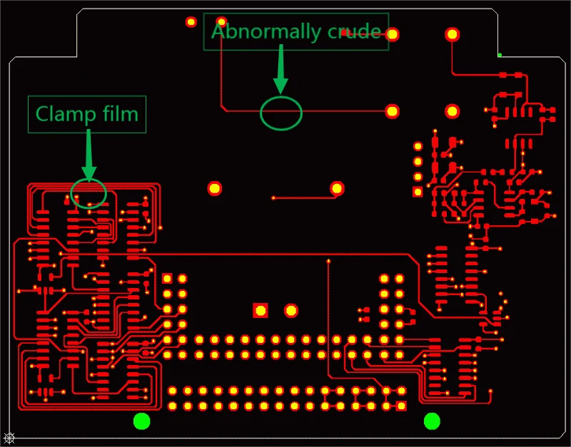
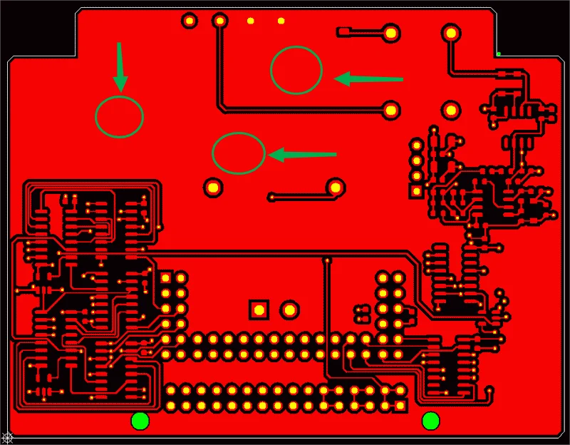
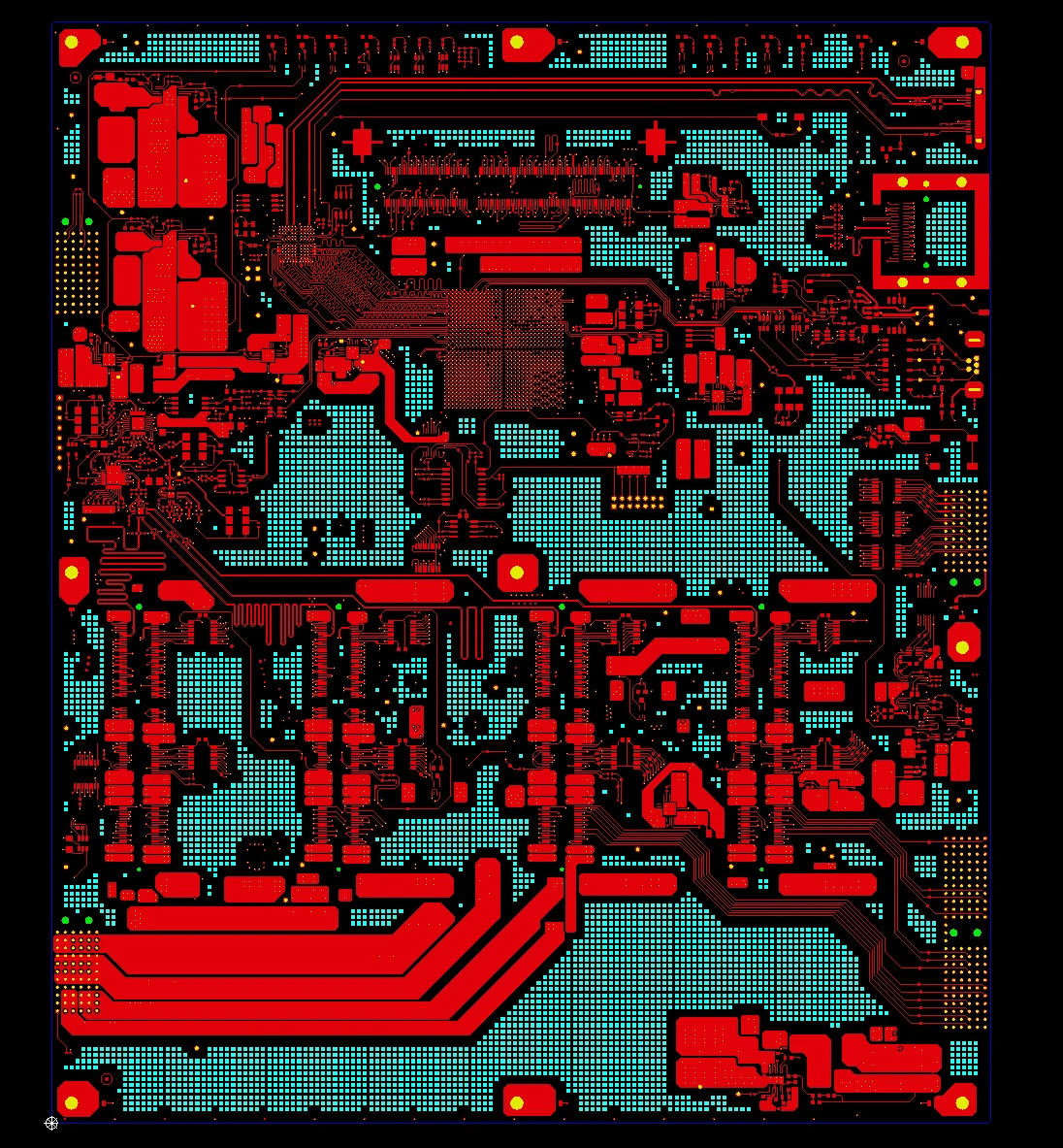
It’s common to see printed circuit board (PCB) designs with large unused, copper-free areas. Often, this stems from a lack of awareness of how these empty spaces can critically impact the PCB manufacturing process and the final product’s reliability. An excessive percentage of unused board area not only compromises performance but can also lead to premature failure, making the design susceptible to early damage.
This is precisely where the practice of PCB copper pouring becomes essential. As a fundamental step in the board production process, copper pouring involves filling these blank areas with a solid or hatched copper plane. While some novice designers might assume that using less copper reduces cost, this is a significant misconception. Although the immediate electroplating area may be smaller, the hidden costs of poor quality and reliability far outweigh the minimal material savings.
At the heart of quality-focused PCB manufacturing, strategic copper pouring is non-negotiable. It significantly enhances product quality by improving signal integrity, thermal management, and mechanical stability. By partnering with a manufacturer that prioritizes robust design-for-manufacturability (DFM) principles, you ensure that adequate copper pouring is implemented to boost your board’s performance and longevity.
What Happens When The Outer Layer Of A PCB Is Copper-Free?
During the electroplating process, the PCB substrate is immersed in the plating bath. When an electrical current is applied, copper is deposited onto the exposed conductive areas not protected by the dry film resist (refer below fig 1).
01: Issue: Unpoured Copper Areas on PCB Outer Layers
This issue can affect a wide range of PCB types, including double-sided PCBs and multilayer boards (4 layers and above).
The exposed copper traces act as a substrate for electrodeposition. During plating, a controlled electrical current reduces copper ions from the solution onto these traces to increase their thickness and conductivity.
During electroplating, the exposed copper acts as a cathode. A small, isolated trace presents a high-resistance path, leading to uneven current density. A large, continuous copper plane provides a low-resistance path, ensuring uniform current reception and consistent copper deposition, as shown in Figure 3.
Problem: Uneven copper area distribution creates plating hotspots. As illustrated in Figure 4, high current density on isolated traces can result in final thickness far exceeding specification (e.g., 2OZ instead of 1OZ).
Excessively narrow trace gaps (e.g., 3-3.5 mil) can trap dry film resist during lamination. This prevents proper etching, leaving conductive copper residue in the gaps and creating a high risk of short circuits, as detailed in Figures 6 and 7.
Solution:
To ensure high manufacturing yield and product reliability, follow these key PCB design and layout rules: First, minimize isolated traces by incorporating copper pours wherever possible. Second, for any necessary isolated traces, maximize the spacing between them to prevent plating and etching defects.
PCB Design Best Practices: A Visual Case Study
- Pouring copper partly
2. Large area without pouring copper
3. Pouring copper by dummy PAD
02 Issue: Unpoured Copper Areas on PCB Inner Layers
This issue primarily affects multilayer PCBs, particularly those with 4 layers or more.
The lamination process is fundamental to multilayer PCB integrity. Prepreg (PP) sheets are layered between cores and foil. When heat and pressure are applied, the PP’s resin melts, fulfilling the critical role of filling all empty spaces in copper-free areas. As it cools and solidifies, it creates a durable dielectric bond that mechanically and electrically unites the entire board stack-up.
1. Excessively large copper-free areas on inner layers cause uncontrolled resin flow from the prepreg (PP). This can result in resin-starved regions, leading to severe quality defects including board thinning, copper foil wrinkling, measling (white spots), and delamination due to insufficient resin in critical areas.
The case is as follows:
2. Insufficient copper backing behind the gold finger area leads to plating thickness issues, resulting in poor electrical contact with the mating connector.
For The Gold Finger Printed Circuit Board:
A solid copper pour is mandatory in the inner layer beneath gold fingers to provide a robust foundation, ensuring proper plating thickness and final board thickness control. Avoid stackups that specify a minimum finished thickness.
Strategically placing copper in inner layer open areas increases copper distribution, reduces resin-filled zones, and enhances lamination reliability and thickness tolerance. On outer layers, copper pouring balances plating current distribution, preventing issues like resist clamping and over-etching of thin traces to achieve uniform surface copper thickness.
03 Summary Of The Design Rules: Critical DFM Guidelines for Copper Pour in PCB Layout
1. Copper Fill & Clearance
• Minimize open areas in the design by filling unused spaces with solid copper.
• Maintain a minimum clearance of 0.5mm between copper pours and tracks, pads, and drill holes.
• Use solid copper pours instead of hatched patterns whenever possible.
2. High-Current & RF Considerations
• For 2 Oz copper designs, ensure a minimum spacing of 8 mils between all features (track-track, track-pad, pad-pad).
• When pouring copper near antenna areas, strictly follow the product design manual to prevent RF interference.
3. Gold Finger Structure
• All inner layers beneath gold fingers must have copper pour to prevent board thinning and ensure structural integrity.
• Avoid laminated structures that specify an excessively thin final board thickness.
Partner with a Professional PCB Manufacturer
As an industry-leading PCB manufacturer, we continuously advance our engineering and manufacturing capabilities to meet the latest high-technology requirements. Contact us anytime for a free project review and quote.