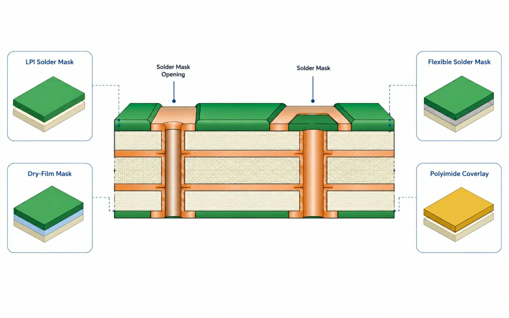
PCB solder mask materials are permanent polymer systems applied over copper to protect the board and control where solder can contact pads. Common options include liquid photoimageable solder mask, dry-film mask, liquid epoxy mask, flexible solder mask, and polyimide coverlay.
In general, most production PCBs use liquid photoimageable solder mask, or LPI, because it supports accurate openings and covers common copper shapes well. However, the correct material still depends on substrate, copper weight, pad geometry, surface finish, assembly temperature, operating environment, color, and the PCB manufacturer’s proven process.
PCB Solder Mask Materials and Main Types
What Is PCB Solder Mask Made Of?
Material and Process Comparison
| Type | Primary Strength | Main Limitation | Typical Use |
|---|---|---|---|
| Liquid photoimageable solder mask | Fine-feature imaging and good conformity | Depends on exposure, development, and cure control | Rigid multilayer, HDI, and most production PCBs |
| Dry-film solder mask | Uniform thickness and fine imaging resolution. | Lamination may be difficult over heavy copper or uneven surfaces. | Used for selected fine-feature PCB and substrate applications. |
| Liquid epoxy or non-LPI mask | Simple application for suitable geometries | Lower imaging resolution than qualified LPI | Less dense or specialized boards |
| Flexible solder mask | Detailed openings with improved bend tolerance | Must be qualified for actual bend conditions | Flexible and rigid-flex circuits |
| Polyimide coverlay | Strong mechanical protection | Adhesive flow and opening accuracy need control | Flex areas requiring durable film protection |
Select the Material by PCB Application
Application-Based Selection Guide

| PCB Condition | Preferred Starting Point | Key Limitation to Confirm |
|---|---|---|
| Standard multilayer FR-4 | Qualified LPI solder mask | Color, finish, cure, and assembly profile |
| Fine-pitch BGA, CSP, or HDI | High-resolution LPI | Minimum dam, registration, and clearance |
| Heavy copper PCB | LPI qualified for high surface relief | Corner coverage and cured thickness |
| Dynamic flex area | Flexible mask or polyimide coverlay | Bend radius, cycle life, and adhesive flow |
| Controlled-impedance RF trace | Mask condition included in field model | Dielectric loading and thickness variation |
| White LED or optical board | Qualified white solder mask | Reflectivity, yellowing, UV stability, and cure |
Properties and Datasheet Validation
Color alone is not a valid solder mask selection criterion. Instead, connect each property to the substrate, copper profile, fabrication process, assembly conditions, and operating environment.
Parameters to Confirm
| Parameter | Why It Matters | Required Evidence |
|---|---|---|
| Cured film thickness | Affects coverage and protection | Measured range over copper and laminate |
| Minimum mask dam | Separates solderable areas | Stable capability by color and process |
| Opening registration | Prevents pad encroachment | Fabricator tolerance and inspection method |
| Final cure profile | Controls hardness and adhesion | Qualified temperature and time window |
| Solder-heat resistance | Reduces reflow or rework damage | Test temperature, duration, and cycle count |
| Electrical properties | May affect leakage or RF behavior | Test method, thickness, frequency, and conditions |
In addition, check the product revision, approved substrates, coating method, storage limits, test methods, qualification references, and limits for each surface finish. However, typical values are not automatically guaranteed acceptance limits.
Substrate, Copper, and RF Effects

For example, FR-4, high-Tg FR-4, polyimide, and RF laminates create different thermal and mechanical demands. Therefore, review the selected PCB base material together with the mask system.
In addition, heavy copper increases surface relief. As a result, coating coverage may become thinner at conductor corners. On controlled-impedance traces, the mask also changes the electrical field around the trace. Therefore, include the intended coverage and thickness in the PCB trace impedance model when tolerance is critical.

PCB Design and DFM Considerations
Therefore, mask openings, pad clearances, registration, and minimum webs must match the selected fabrication process. In addition, WellerPCB recommends confirming these features and via treatments during DFM review.
Openings, Clearances, and Mask Dams
SMD, NSMD, and Via Treatment

Common Manufacturability Risks
- Using one clearance rule for every manufacturer
- Designing dams below stable production capability
- Confusing solder mask openings with stencil apertures
- Ignoring registration around fine-pitch pads
- Leaving unintended openings over traces or copper
- Applying rigid-board rules inside active flex areas
Fabrication, Surface Finish, and Assembly Effects
Application and Cure Process
- Clean and prepare the copper surface.
- Apply the qualified coating method.
- Dry, expose, and image the pattern.
- Develop the panel to remove uncured material.
- Complete final cure and inspect the coating.

Therefore, control surface cleanliness, exposure, development, and final cure. Otherwise, the board may develop weak adhesion, poor openings, pinholes, or later assembly defects.
Surface Finish and PCBA Compatibility
For example, ENIG, HASL, OSP, immersion silver, and immersion tin use different chemical or thermal steps. Therefore, confirm compatibility with the selected PCB surface finish.
In addition, mask geometry can affect solder bridging, paste behavior near pad edges, BGA or QFN pad definition, reflow exposure, and inspectability. By contrast, the paste-mask layer defines stencil apertures and is not the fabricated solder mask. Therefore, coordinate the design with the planned PCB assembly process.
Quality Control, Standards, and Defect Risks
Common Defects and Checks
| Defect | Possible Cause | Recommended Check |
|---|---|---|
| Peeling or blistering | Contamination, moisture, poor preparation, or inadequate cure | Adhesion, preparation records, and cure conditions |
| Pinholes or skips | Poor coverage, contamination, or surface relief | Visual or optical inspection |
| Pad encroachment | Registration, compensation, or artwork error | CAM data and opening measurements |
| Missing mask dam | Designed web below process capability | DFM review and finished-feature inspection |
Standards and Documentation
If UL recognition is required, confirm that the specific material and board construction are covered. In addition, RoHS and REACH declarations may be required. However, these documents do not replace inspection or process records.
Testing Scope
By contrast, X-ray, ICT, flying probe, electrical testing, and functional testing evaluate other PCB or PCBA risks; they do not qualify the solder mask coating. Similarly, assembly AOI checks visible components and solder joints. Therefore, define mask-specific checks in the PCB manufacturing quality plan.

How to Specify and Source Solder Mask Material
Therefore, a clear RFQ reduces assumptions and helps the manufacturer review material, design, compliance, cost, and scheduling risks before release.
Information to Include
- Required color, gloss, and appearance
- Approved product or functional requirements
- Thermal, electrical, chemical, optical, or flex needs
- Controlled openings and via-treatment requirements
- Acceptance standards and compliance documents
- Lot traceability or certificate requirements
- Restrictions on equivalent-material substitution
Cost and Lead-Time Drivers
Prototype-to-Production Control
Select the Mask by Board, Process, and Product Risk
Select PCB solder mask materials by matching their cured properties and imaging capability to the substrate, copper geometry, pad design, surface finish, assembly profile, and operating environment. Confirm actual process limits and validate the finished coating through inspection.
Frequently Asked Questions
How thick should PCB solder mask be?
Can solder mask cover or tent vias?
Is black solder mask harder to inspect than green?
It can be. Dark surfaces may reduce visual or optical contrast. Confirm imaging, AOI, registration, and cosmetic capability before using black mask on dense layouts.