However, the final construction still depends on controlled-impedance targets, finished copper, board thickness, component density, EMC and power requirements, laminate selection, and fabrication capability. Accordingly, this guide covers layer order, reference-plane design, impedance geometry, standard 4-layer constructions, heavy copper, prepreg, and the manufacturing variables that should be confirmed before routing or production release.
Structure and Layer Functions
| Layer | Typical Function | Design Purpose |
|---|---|---|
| L1 | Top Signal / Components | Components and critical routing |
| L2 | Ground Plane | Continuous signal reference and return path |
| L3 | Power Plane | Power distribution and selected low-risk routing |
| L4 | Bottom Signal | Secondary routing and components |
Compared with a 2-layer PCB, dedicated internal planes can improve return-path continuity, reduce loop area, simplify power distribution, and make controlled-impedance routing more practical. These benefits depend on layout quality; adding two layers alone does not correct poor reference-plane design.
Recommended 4-Layer PCB Layer Order
Practical starting point for many general-purpose designs.
Consider for EMC-sensitive designs where outer ground layers are useful.
Use more layers when four layers cannot preserve routing and reference-plane margin.
Reference Planes and Signal Integrity in a 4-Layer PCB

Controlled Impedance in a 4-Layer PCB Stackup
A 50Ω trace has no universal width. Trace geometry must be calculated from the actual dielectric height, finished copper, material properties, and approved production stackup.
Consequently, use the production stackup approved by the PCB manufacturer for impedance calculations. WellerPCB’s PCB controlled impedance guide covers the relationship between stackup geometry, calculation, manufacturing variation, and verification.
For additional industry guidance, see the IPC-2141A controlled-impedance design guide.
WellerPCB 4-Layer PCB Stackup Thickness Options

4L PCB Stack-Up T=0.50mm
| Layer | T: um | Material | |||||
| SMT | Soldermask | 20 | Solder rmask | ||||
| TOP | 1 | Copper | 18-25 | Copper plating | |||
| 18 | Base copper | ||||||
| Prepreg | 2116X1 | 105 | Prepreg | ||||
| INT1 | 2 | Copper | 35 | Copper | |||
| Core | FR4 | 130 | Core | ||||
| INT2 | 3 | Copper | 35 | Copper | |||
| Prepreg | 2116X1 | 105 | Prepreg | ||||
| BOT | 4 | Copper | 18 | Base copper | |||
| 18-25 | Copper plating | ||||||
| SMB | Soldermask | 20 | Solder rmask | ||||
| Finished PCB thickness: 0.5+/-0.10mm | |||||||
4L PCB Stack-Up T=0.80mm
| Layer | T: um | Material | |||||
| SMT | Soldermask | 20 | Solder rmask | ||||
| TOP | 1 | Copper | 18-25 | Copper plating | |||
| 18 | Base copper | ||||||
| Prepreg | 1080X1 | Prepreg | |||||
| 7628X1 | |||||||
| INT1 | 2 | Copper | 35 | Copper | |||
| Core | FR4 | 175 | Core | ||||
| INT2 | 3 | Copper | 35 | Copper | |||
| Prepreg | 7628X1 | Prepreg | |||||
| 1080X1 | |||||||
| BOT | 4 | Copper | 18 | Base copper | |||
| 18-25 | Copper plating | ||||||
| SMB | Soldermask | 20 | Solder rmask | ||||
| Finished PCB thickness: 0.8+/-0.10mm | |||||||
4L PCB Stack-Up T=1.00mm
| Layer | T: um | Material | |||||
| SMT | Soldermask | 20 | Solder rmask | ||||
| TOP | 1 | Copper | 18-25 | Copper plating | |||
| 18 | Base copper | ||||||
| Prepreg | 1080X1 | Prepreg | |||||
| 7628X1 | |||||||
| INT1 | 2 | Copper | 35 | Copper | |||
| Core | FR4 | 440 | Core | ||||
| INT2 | 3 | Copper | 35 | Copper | |||
| Prepreg | 7628X1 | Prepreg | |||||
| 1080X1 | |||||||
| BOT | 4 | Copper | 18 | Base copper | |||
| 18-25 | Copper plating | ||||||
| SMB | Soldermask | 20 | Solder rmask | ||||
| Finished PCB thickness: 1.00+/-0.10mm | |||||||
4L PCB Stack-Up T=1.60mm
| Layer | T: um | Material | |||||
| SMT | Soldermask | 20 | Solder rmask | ||||
| TOP | 1 | Copper | 18-25 | Copper plating | |||
| 18 | Base copper | ||||||
| Prepreg | 1080X1 | Prepreg | |||||
| 7628X1 | |||||||
| INT1 | 2 | Copper | 35 | Copper | |||
| Core | FR4 | 930 | Core | ||||
| INT2 | 3 | Copper | 35 | Copper | |||
| Prepreg | 7628X1 | Prepreg | |||||
| 1080X1 | |||||||
| BOT | 4 | Copper | 18 | Base copper | |||
| 18-25 | Copper plating | ||||||
| SMB | Soldermask | 20 | Solder rmask | ||||
| Finished PCB thickness: 1.60+/-0.16mm | |||||||
4L PCB Stack-Up T=2.00mm
| Layer | T: um | Material | |||||
| SMT | Soldermask | 20 | Solder rmask | ||||
| TOP | 1 | Copper | 18-25 | Copper plating | |||
| 18 | Base copper | ||||||
| Prepreg | 1080X1 | Prepreg | |||||
| 7628X1 | |||||||
| INT1 | 2 | Copper | 35 | Copper | |||
| Core | FR4 | 1530 | Core | ||||
| INT2 | 3 | Copper | 35 | Copper | |||
| Prepreg | 7628X1 | Prepreg | |||||
| 1080X1 | |||||||
| BOT | 4 | Copper | 18 | Base copper | |||
| 18-25 | Copper plating | ||||||
| SMB | Soldermask | 20 | Solder rmask | ||||
| Finished PCB thickness: 2.00+/-0.20mm | |||||||
4L PCB Stack-Up T=2.50mm
| Layer | T: um | Material | |||||
| SMT | Soldermask | 20 | Solder rmask | ||||
| TOP | 1 | Copper | 18-25 | Copper plating | |||
| 18 | Base copper | ||||||
| Prepreg | 1080X1 | Prepreg | |||||
| 7628X1 | |||||||
| INT1 | 2 | Copper | 35 | Copper | |||
| Core | FR4 | 1930 | Core | ||||
| INT2 | 3 | Copper | 35 | Copper | |||
| Prepreg | 7628X1 | Prepreg | |||||
| 1080X1 | |||||||
| BOT | 4 | Copper | 18 | Base copper | |||
| 18-25 | Copper plating | ||||||
| SMB | Soldermask | 20 | Solder rmask | ||||
| Finished PCB thickness: 2.50+/-0.25mm | |||||||
4L PCB Stack-Up T=3.00mm
| Layer | T: um | Material | |||||
| SMT | Soldermask | 20 | Solder rmask | ||||
| TOP | 1 | Copper | 18-25 | Copper plating | |||
| 18 | Base copper | ||||||
| Prepreg | 1080X1 | Prepreg | |||||
| 7628X1 | |||||||
| INT1 | 2 | Copper | 35 | Copper | |||
| Core | FR4 | 2330 | Core | ||||
| INT2 | 3 | Copper | 35 | Copper | |||
| Prepreg | 7628X1 | Prepreg | |||||
| 1080X1 | |||||||
| BOT | 4 | Copper | 18 | Base copper | |||
| 18-25 | Copper plating | ||||||
| SMB | Soldermask | 20 | Solder rmask | ||||
| Finished PCB thickness: 3.00+/-0.30mm | |||||||
Heavy-Copper 4-Layer PCB Stackup

4L PCB Stack-Up T=1.60mm, 2/2/2/2oz, Option-1
| Layer | T: um | Material | |||||
| SMT | Soldermask | 20 | Solder rmask | ||||
| TOP | 1 | Copper | 25-35 | Copper plating | |||
| 35 | Base copper | ||||||
| Not the best option | Prepreg | 7628X1 | Prepreg | ||||
| 7628HX1 | |||||||
| INT1 | 2 | Copper | 70 | Copper | |||
| Core | FR4 | 460 | Core | ||||
| INT2 | 3 | Copper | 70 | Copper | |||
| Not the best option | Prepreg | 7628HX1 | Prepreg | ||||
| 7628X1 | |||||||
| BOT | 4 | Copper | 35 | Base copper | |||
| 25-35 | Copper plating | ||||||
| SMB | Soldermask | 20 | Solder rmask | ||||
| Finished PCB thickness: 1.60+/-0.16mm | |||||||
4L PCB Stack-Up T=1.60mm, 2/2/2/2oz, Option-2
| Layer | T: um | Material | |||||
| SMT | Soldermask | 20 | Solder rmask | ||||
| TOP | 1 | Copper | 25-35 | Copper plating | |||
| 35 | Base copper | ||||||
| The best option | Prepreg | 1080 (RC 60%) | 76 | Prepreg | |||
| 7628 (RC 48%) | 220 | ||||||
| INT1 | 2 | Copper | 70 | Copper | |||
| Core | FR4 | 830 | Core | ||||
| INT2 | 3 | Copper | 70 | Copper | |||
| The best option | Prepreg | 7628 (RC 48%) | 220 | Prepreg | |||
| 1080 (RC 60%) | 76 | ||||||
| BOT | 4 | Copper | 35 | Base copper | |||
| 25-35 | Copper plating | ||||||
| SMB | Soldermask | 20 | Solder rmask | ||||
| Finished PCB thickness: 1.60+/-0.16mm | |||||||
Prepreg, Resin Content, and Dielectric Constant
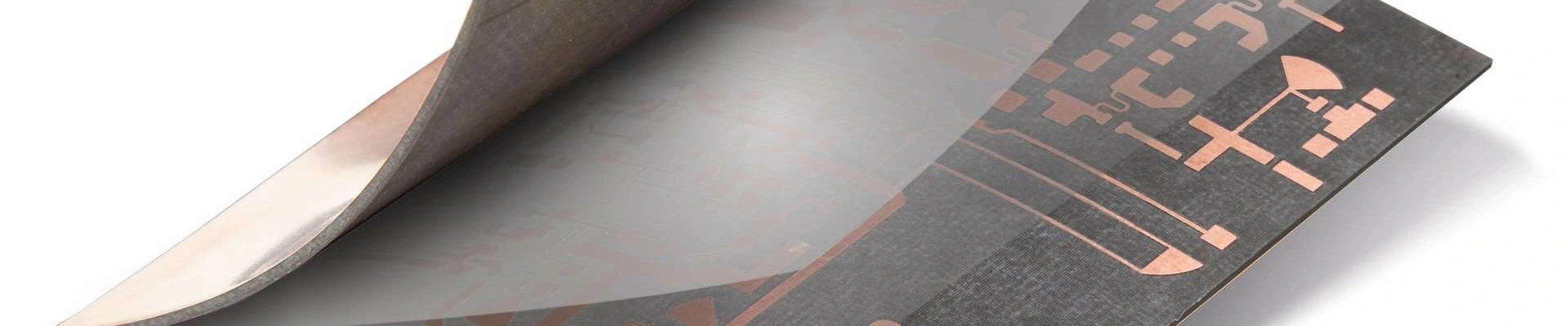
First, during multilayer lamination, prepreg forms the bonding dielectric. Its final pressed thickness depends on glass style, resin content, copper thickness, copper pattern, and lamination conditions. As a result, common constructions such as 1080, 2116, and 7628 should not be assumed to have identical physical or electrical behavior.
Based Material Line Up S1000H (S1000HB)-PREPREG (B-STAGE)
| Glass style | RC (%) Nominal | Thickness | Dk | Df | |||||||
| mm | mil | 1GHz | 3GHz | 5GHz | 10GHz | 1 GHz | 3 GHz | 5 GHz | 10 GHz | ||
| 7628 | 43* | 0.185 | 7.28 | 4.81 | 4.74 | 4.74 | 4.73 | 0.014 | 0.015 | 0.015 | 0.016 |
| 7628 | 46 | 0.195 | 7.68 | 4.74 | 4.68 | 4.66 | 4.66 | 0.015 | 0.016 | 0.016 | 0.016 |
| 7628 | 48 | 0.205 | 8.07 | 4.70 | 4.63 | 4.61 | 4.61 | 0.015 | 0.016 | 0.016 | 0.017 |
| 7628 | 50 | 0.215 | 8.46 | 4.65 | 4.58 | 4.57 | 4.57 | 0.016 | 0.016 | 0.017 | 0.017 |
| 7628 | 52 | 0.225 | 8.86 | 4.59 | 4.52 | 4.51 | 4.50 | 0.016 | 0.016 | 0.017 | 0.017 |
| 1506 | 48 | 0.160 | 6.30 | 4.70 | 4.63 | 4.61 | 4.61 | 0.015 | 0.016 | 0.016 | 0.017 |
| 1506 | 50 | 0.170 | 6.69 | 4.65 | 4.58 | 4.57 | 4.57 | 0.016 | 0.016 | 0.017 | 0.017 |
| 1506 | 52 | 0.180 | 7.09 | 4.59 | 4.52 | 4.51 | 4.50 | 0.016 | 0.016 | 0.017 | 0.017 |
| 2116 | 52* | 0.113 | 4.45 | 4.59 | 4.52 | 4.51 | 4.50 | 0.016 | 0.016 | 0.017 | 0.017 |
| 2116 | 53* | 0.116 | 4.57 | 4.57 | 4.50 | 4.49 | 4.48 | 0.016 | 0.017 | 0.017 | 0.018 |
| 2116 | 55 | 0.120 | 4.72 | 4.53 | 4.45 | 4.43 | 4.43 | 0.017 | 0.017 | 0.018 | 0.018 |
| 2116 | 58 | 0.130 | 5.12 | 4.45 | 4.38 | 4.36 | 4.36 | 0.017 | 0.018 | 0.018 | 0.018 |
| 3313 | 57 | 0.100 | 3.94 | 4.48 | 4.41 | 4.39 | 4.39 | 0.017 | 0.018 | 0.018 | 0.018 |
| 1080 | 65 | 0.072 | 2.83 | 4.29 | 4.21 | 4.19 | 4.18 | 0.019 | 0.019 | 0.019 | 0.020 |
| 1080 | 68 | 0.081 | 3.19 | 4.21 | 4.13 | 4.11 | 4.11 | 0.020 | 0.019 | 0.020 | 0.020 |
| 1080 | 70 | 0.087 | 3.43 | 4.16 | 4.08 | 4.05 | 4.05 | 0.020 | 0.019 | 0.020 | 0.020 |
| 106 | 73 | 0.050 | 1.97 | 4.09 | 4.01 | 3.97 | 3.97 | 0.020 | 0.020 | 0.020 | 0.020 |
| 106 | 78 | 0.063 | 2.14 | 3.97 | 3.89 | 3.83 | 3.83 | 0.02 | 0.021 | 0.020 | 0.022 |
| Remark: | |||||||||||
| 1) Test by SPDR method. | |||||||||||
| 2) The data above show actual values and are not guaranteed, for your reference only. | |||||||||||
| 3) RC* is not common type for reference. | |||||||||||
| 4) Last update: Oct, 2025 | |||||||||||
Copper Weight and Finished Copper Thickness
When to Ask WellerPCB for a Custom 4-Layer Stackup

Power Integrity and EMC in a 4-Layer PCB
Finally, for EMC, keep high-speed signals close to continuous reference planes, minimize high-frequency current-loop area, avoid unnecessary plane slots, and provide appropriate return paths around signal-layer transitions.
Common 4-Layer PCB Stackup Mistakes
- Choosing the stackup after routing: define the preliminary construction before critical routing and impedance work.
- Assuming every 1.6 mm board has the same geometry: total thickness does not define signal-to-plane spacing.
- Routing across plane splits: a broken return path can increase loop area and create SI or EMI problems.
- Treating FR-4 as one fixed Dk: laminate system, glass style, resin content, frequency, and test method affect electrical properties.
- Ignoring finished copper: plating changes conductor thickness and profile.
- Forcing dense routing into four layers: additional layers can be preferable to sacrificing plane continuity or manufacturing margin.
4-Layer PCB Stackup Design Checklist
4-Layer PCB Stackup FAQ
What is the most common 4-layer PCB stackup?
A common arrangement is Signal / Ground / Power / Signal. It gives top-layer routing a nearby ground reference and provides a practical starting point for many products.