
Introduction to Heavy Copper PCBs
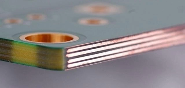
Heavy copper PCB (typically 3oz to 20oz copper weight) represent a critical advancement in printed circuit board technology, enabling unprecedented current-carrying capacity and thermal management for power electronics. Unlike standard PCBs (with 1-2oz copper weight), these robust boards can handle 100+ amps per layer, making them indispensable in high-power applications from electric vehicles to industrial power systems.
At WELLER, we’ve manufactured heavy copper boards for mission-critical applications where reliability under extreme conditions is non-negotiable. This comprehensive guide explores the design, manufacturing, and application considerations for these engineering powerhouses.
Why Heavy Copper PCBs? Key Advantages
Enhanced Current Capacity
- 3-5X higher ampacity than standard PCBs
- Supports 100-500A current loads (vs. 10-30A for standard boards)
Superior Thermal Management
- Copper's 401 W/m·K thermal conductivity dissipates heat efficiently
- Reduces hot spots by 40-60% compared to standard designs
Increased Mechanical Strength
- Reinforced plated through-holes withstand 10,000+ thermal cycles
- Eliminates need for external busbars in power converters
Space Optimization
- Single heavy copper layer replaces multiple standard layers
- 60% space reduction in EV battery management systems
Critical Applications Driving Demand
Automotive & EV Systems
- EV charging stations (50kW-350kW)
- Battery management systems (400V/800V architectures)
- DC-DC converters for electric drivetrains
Industrial Power Electronics
- Motor drives (1-100HP)
- Motor drives (1-100HP)
- Uninterruptible power supplies (UPS)
- Welding equipment controllers
Renewable Energy Infrastructure
- Solar inverters (micro to utility-scale
- Wind turbine power converters
- Grid-scale energy storage system
Aerospace & Defense
- Avionic power distribution
- Radar transmitter modules
- Satellite power systems
Heavy Copper PCB Design Rules (DFM Guidelines)
Trace Width & Spacing Requirements
| Copper Weight (OZ) | Min Trace Width (mil/mm) | Min Spacing (mil/mm) | Current Capacity (Amp)(ΔT=20°C) |
| 0.33 | 3.50/0.089 | 3.00/0.08 | 0.25 |
| 0.50 | 4.00/0.10 | 3.50/0.089 | 0.38 |
| 1.00 | 6.00/0.15 | 5.50/0.14 | 0.65 |
| 2.00 | 7.00/0.18 | 7.00/0.18 | 1.03 |
| 3.00 | 8.00/0.2 | 10.00/0.25 | 25 |
| 6.00 | 12.00/0.30 | 13.78/0.35 | 50 |
| 10.00 | 20.00/0.50 | 23.60/0.60 | 85 |
| 20.00 | 40.00/1.00 | 47.20/1.20 | 180 |
| *Per 10mm trace length at 20°C temperature rise | |||
Via Design Considerations
- Aspect ratio ≤ 8:1 (e.g., 0.3mm drill for 2.4mm board)
- Plated copper thickness ≥ 25μm (IPC Class 3 standard)
- Via filling with conductive/epoxy for thermal paths
Thermal Relief Best Practices
KiCAD Thermal Relief Settings
(thermal_gap 0.25mm)
(thermal_spoke_width 0.4mm)
(thermal_spoke_count 4)
Prevents solder wicking during assembly
Material Selection Considerations
- High TG substrates (>170°C): FR4-TG170, Polyimide
- Low CTE laminates: ≤50 ppm/°C (z-axis)
- Thermal interface materials: Ceramic-filled prepregs
Heavy Copper PCB Manufacturing Process: Step-by-Step
Material Preparation
- Copper-clad laminates with 3-20oz base foil
- Laser direct imaging (LDI) for precise pattern transfer
Pattern Plating Technology
- Step 1: Initial copper deposition (5-8μm)
- Step 2: Pulse plating for uniform thickness distribution
- Step 3: Controlled current density (15-25 ASF)
Differential Etching
- Acid copper etchants (CuCl₂/HCl)
- Temperature control: 50±2°C
- Etch factor > 3:1 (critical for 20oz traces)
Thermal Management Features
- Embedded copper coins
- Copper-filled vias
- Thermal vias arrays under power components </ul
Quality Validation
- Automated optical inspection (AOI) for trace integrity
- X-ray thickness measurement (copper weight verification)
- Thermal cycling tests(-55°C to +150°C, 1000 cycles)

Weller PCB's Heavy Copper Manufacturing Capabilities
Technical Specifications
| Parameter | Capability |
| Max Copper Weight | 20oz (700μm) |
| Layer Count | 2-24 Layer |
| Min Trace/Space | 0.15mm/0.20mm (for 3oz) |
| Board Thickness | 0.4mm – 7.0mm |
| Surface Finishes | ENIG, HASL, Immersion Silver, OSP |
Industry Certifications
- IPC-6012 Class 3 (High Reliability)
- IATF 16949 (Automotive Standard)
- UL Recognition

Choosing the Right Heavy Copper PCB Manufacturer
Not all PCB fab houses can produce reliable Heavy Copper boards. Look for a partner with:
Proven Expertise:
A portfolio of successful projects and specific experience with your required copper weight.
Advanced Equipment:
Access to specialized plating lines, etching systems, and lamination presses capable of handling thick copper.
Design for Manufacturability (DFM) Support:
A team that will review your designs early and provide feedback on trace width, spacing, and aspect ratios to prevent costly errors.
Rigorous Quality Control:
Certifications (e.g., ISO 9001, AS9100) and a clear commitment to testing and inspection.
Conclusion
Heavy Copper PCB technology is the backbone of modern high-power electronics, enabling the robust and compact designs demanded by industries from renewable energy to electric vehicles. Understanding the unique design rules and complex manufacturing processes is key to leveraging their full potential.
By partnering with an experienced manufacturer and applying the principles outlined in this guide, you can ensure your next high-power project is built on a foundation of strength, reliability, and performance.
Ready to Power Up Your Next Project?
WELLER specializes in advanced PCB manufacturing, including complex Heavy Copper and Extreme Copper designs up to 20oz+. Get an Instant Quote today or Contact Our Engineering Team for a free DFM review.


