
Bow and twist are two critical types of deformation that can occur during or after the PCB manufacturing process, directly impacting the flatness (or warpage) of a finished board as defined by the IPC-600 standard.
Bow refers to a curvature where the center of the PCB is either raised or lowered relative to its edges, forming a gentle arc. Twist, on the other hand, occurs when one corner of the board is lifted or lowered relative to the other three, resulting in a distorted, non-coplanar surface.
Advancements in component technology — particularly the widespread adoption of Surface Mount Technology (SMT) and finer-pitch components — are driving demand for higher-density interconnections, tighter tolerances, and superior PCB flatness. In some advanced applications, the PCB itself serves as an SMT component that must be mounted onto another board, making controlled bow and twist essential for reliable assembly.
Failure to control bow and twist can severely compromise the reliability and performance of the final PCBA, making it imperative for electronics designers to specify strict flatness requirements for applications where perfection is non-negotiable.


The continuing miniaturization of SMT components and the advancement of high-density interconnects (HDI) have dramatically increased the challenges of controlling PCB bow and twist. This article examines the root causes of these defects—both intrinsic and extrinsic—and provides actionable strategies for designers and manufacturers to enhance PCB flatness, ensure compliance with IPC standards, and improve overall board reliability and performance.
What is the Bow and Twist in PCBs
Bow and twist refer to deformations in a printed circuit board (PCB) that compromise its flatness, ultimately affecting both assembly yield and end-product performance. These defects stem from a combination of intrinsic (built-in) and extrinsic (external) factors introduced during design, manufacturing, or handling.
The root causes of bow and twist are categorized as either intrinsic or extrinsic. Intrinsic factors originate before or during the lamination cure process. These are often baked into the board and are difficult or impossible to correct later. Common examples include an unbalanced copper distribution across layers or an asymmetric stack-up structure. Extrinsic factors occur after lamination, due to subsequent manufacturing steps, environmental stress, or handling. These often allow for some corrective action.
Understanding what drives these deformations is critical for prevention. The following sections detail how specific issues in PCB layout design, production processes, and external forces directly influence a board’s susceptibility to bow and twist.
Production related intrinsic reasons:
- Layer lamination press malfunction.
- Cross plying prepreg or inner layers – warp and fill directions must be same (Latitude and longitude).
- Wrong glass ply construction used (Prepreg or Cores).
- Missing or extra prepreg glass ply.
- Weave distortion or deformed (Cores or Prepreg).
- Inner layers Not fully cured.
Design related intrinsic reasons:
- Unsymmetrical stack-up design (Prepreg and/or Cores).
- Unbalanced copper distribution in circuit layer.
- Unbalanced copper distribution in circuit layer.
- Within layers causing low pressure areas.
- Core constructions.
- Breakaway area not matching copper distribution per layer.
- Too big PCB size (the bigger size the harder control in the flatness).
- Too thin PCB thickness (the thinner thickness, the easier in twist).
External related extrinsic reasons:
- Mechanical deformation.
- Unproperly handling.
- Heat impacting during the solder mask or legend cure step.
- High temperature in HASL process.
- Reflow in PCB assembly process.
The More You Need To Know
The copper dummy PAD design in the breakaway tab should have the similar copper distribution for each layer. As long as breakaway area is perfectly copper balanced, it will behave differently from the non-perfect PCB, causing potential stress that could lead to a twist in the PCB panel, especially when separating the PCB from the breakaway tabs.
Copper Pour vs. No Copper Pour in PCB Manufacturing


How to Measure Bow and Twist in PCBs: Procedures and Standards
To ensure superior board flatness, PCB manufacturers must implement rigorous testing throughout production to minimize intrinsic bow and twist. When boards exhibit excessive warpage after delivery, determining whether the root cause is intrinsic (manufacture-based) or extrinsic (assembly or handling-related) becomes critical for effective resolution. Follow this standardized measurement procedure to accurately diagnose and address PCB deformation issues.
Recommended Measurement Procedure:
Initial Measurement:
Perform initial bow and twist evaluation according to IPC-TM-650 2.4.22 method.
Baking Process:
Bake the boards at a temperature 10°C above the material's Tg value for 20 minutes. Place them flat on a level surface, ensuring no boards are stacked or touching.
Controlled Cooling:
Cool the boards to room temperature inside the closed oven at a controlled rate of 1°C per minute to prevent thermal shock.
Final Measurement:
Re-measure bow and twist using IPC-TM-650 2.4.22 method after boards reach room temperature.
Results Interpretation:
If PCBs become completely flat:
The root cause was purely extrinsic (temporary stress)
If PCBs remain unchanged:
The root cause is purely intrinsic (manufacturing-related)
If deformation improves but persists:
The issue represents a mix of intrinsic and extrinsic factors
The delta value between initial and final measurements quantifies the combined intrinsic and extrinsic deformation components, providing valuable data for process improvement and quality control.
Bow and Twist Improvements
When it comes to address bow and twist issues that exceed required tolerances, we must thoroughly investigate the underlying intrinsic causes and fine-tune both design and production aspects that probably impact performance.
At first, we must ensure that all relevant production processes are properly under control.
And then, we need to review potential improvements and corrections in the manufacturing process that could improve performance beyond standard expectations.
The delta value between initial and final measurements quantifies the combined intrinsic and extrinsic deformation components, providing valuable data for process improvement and quality control.
Lamination process
The lamination in PCB manufacturing process is normally tuned to be cost effective and still meet required tolerances. The pressing cycle can be tuned further through extending the cycle times to achieve improved performance.

Prepreg and inner cores
The PCB manufacturer has to find a tradeoff of the use of prepreg between a customer’s specifications and the optimal choice for high performance. To achieve improved stability, the buildup must be 100% symmetric, and the PCB fabrication house need to choose the most robust prepregs and core constructions. The result will more or less affect impedance that needs to be recalculated.
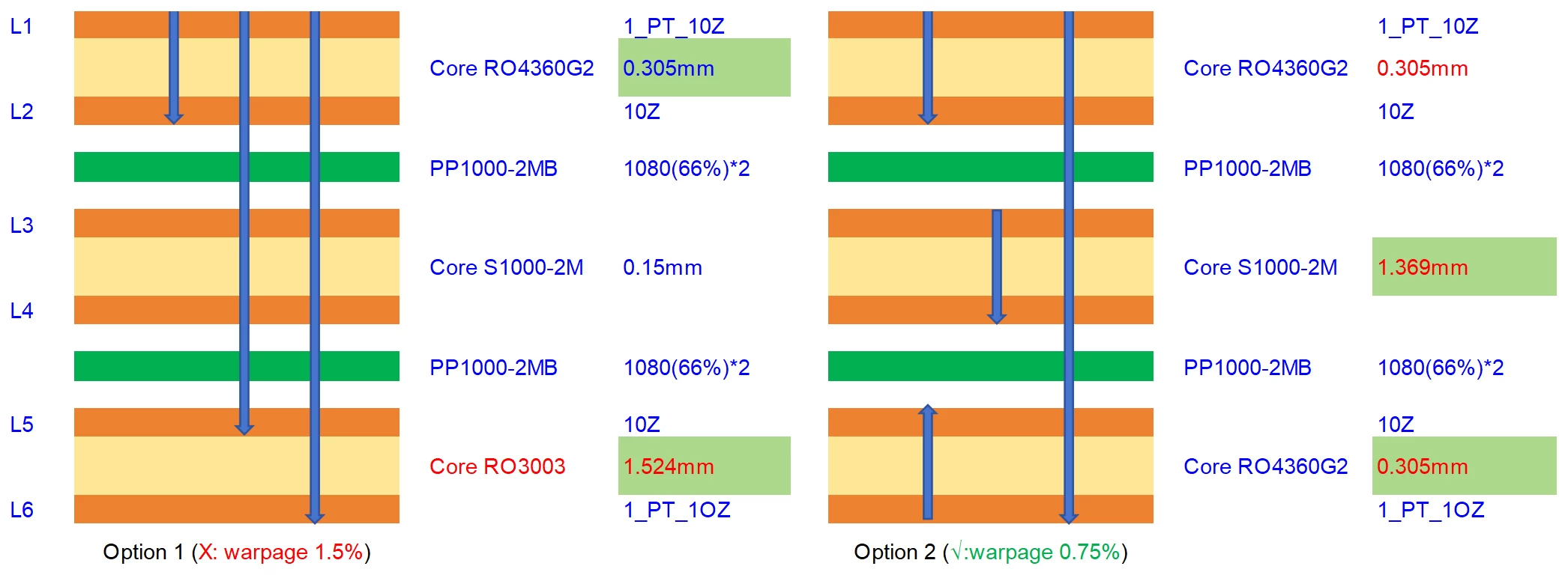
Refer below 2 options stackup comparison for a 6 layer HDI PCB board:
Option 1 is an unsymmetrical stackup structure in drill process (d1-d2; d1-d5, d1-d6); and core thickness L1-L2: 0.305mm, L6-L5:1.5mm. This would have a poor circuit board warpage 1.5% or even higher.
Option 2 is a symmetrical stackup structure both in drill process (d1-d2; d2-d5, d5-d6); and core thickness L1-L2: 0.305mm, L6-L5: 0.305mm. This would have a perfect circuit board warpage 0.75%(max).
Copper distribution
Copper distribution must be optimized within each circuit layer (power and ground layer) and should be matched within the buildup. The buildup must be symmetric and all pairs of layers on each side of the buildup center should have equal copper weight.
Low-pressure areas
Most designs with a high layer count will have a tendency of low-pressure areas. This could be avoided by adding copper pouring by dummy pads or cross hatched copper.
Split ground planes
Some PCB designs have some layers with so-called split planes that may perform as a bend indicator line, especially if the design have the same pattern in more than one layer through the buildup.
Breakaway areas
The PCB breakaway tab is crucial and the most neglected reason for bow and twist. It is very important for the performance that the coppery on each layer breakaway tab imitate the copper of the PCB itself.
The bow and twist managing for improved PCB performance is a complex work that includes all of above considerations. Monitoring which actions yield the desired effect may need several sample runs. Furthermore, various measures can be performed during the waving soldering and reflow assembly process to improve flatness.
With the support of our experienced technicians and engineers, we possess the expertise and knowledge to support our customers toward achieving superior performance. For assistance with a top bow and twist design, please contact us freely, our experienced engineer will response positively.


