Skip to content
  • PCB Layout & Design
    Capability
    • Advantages
    • Design Capability
    • Process
    Solution
    • Reverse Engineering
    • Coplanar Desgin
    Calculator
    • PCB Trace Width
    • Via Current
    • Impedance
      • Microstrip
      • Embedded Microstrip
      • Edge Coupled Microstrip
      • Stripline
      • Asymmetric Stripline
      • Broadside Coupled Stripline
      • Edge Coupled Stripline
    Learn About
    • FAQ
    • Quote
  • PCB Fabrication
    Capability
    • Multilayer
    • HDI
    • Flex PCB
    • Rigid-flex
    • Process
    • Base Material
    • Surface Finishes
    • Equipments
    • Quick Turn
    Solution
    • DFM
    • Heavy Copper
    • Via in Pad
    • Emdedded Coin
    • Stack up
    • Hybrid PCB
    • Countersink Hole
    • Halogen Free
    • Ioni Contamination
    • Chemical Test
    • IPC Class 2 3
    • Quality Assurance
    Learn About
    • Altium Designer
    • Eagle PCB
    • Flex
    • PCB Quote
  • PCB Assembly
    Capability
    • SMT
    • Process
    Solution
    • AOI
    • X-ray
    • Firmware & Testing
    • Conformal Coating
    • Encapsulation & Potting
    • Debug & Repair
    • Wiring Bonding
    • Underfill
    • Turnkey Solution
    Learn About
    • Quote
  • Our Services
    Engineering
    • Advanced Engineering Services
    Manufacturing
    • EMS
    • Box Building Assembly
    • Rapid Prototyping
    • NPI
    • Cable Harness Mfg. & Assembly
    • CNC Machining
    • Ultrasonic Welding
    • Prototype Molding
    • Injection Molding
    • 3D Printing
    Supply Chain
    • Solutions
    • In Stock
  • Products
  • Case Studies
  • About Us
    • About Weller
    • Why Us
    • Agent Wanted
    • Compliance
    • Warranty
    • Terms & Conditions
      • Standard Terms
      • Supplier Terms
      • Supplier Quality Requirements
      • Specification for Printed Circuit Boards
      • Conflict Minerals Policy
    • Testimonials
    • Holiday Shipping Schedule
    • Latest Blogs
  • Contact
Quote

Day: January 20, 2025

PCB Warpage Control: Mitigating Bow and Twist in Printed Circuit Board Manufacturing

PCB board showing bow and twist deformation, a common manufacturing defect affecting flatness.

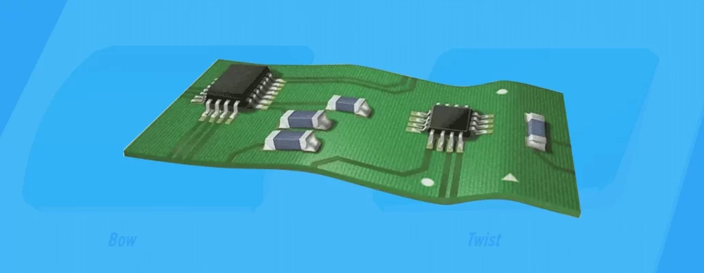
Bow and twist on a bare printed circuit board are two types of deformations that can occur during and after the PCB manufacturing process.

Complete Project

Contact Us Now for Immediate Project Assistance

Address

CN: 4/F, Bldg.3, Huafeng Longgang Overseas Returnees Ind. Park, Baolong lst Rd, Nanyue Cmty, Baolong St, Longgang Dist., Shenzhen, China. 518116

US: 407 Flemington Road,Huntsville,AL 35802, U.S.A.

EU: Z.A.Buisson de la Couldre 8, allée des Châtaigniers 78190 Trappes France.

Phone

+86 755 2828 2776

Email

[email protected]

Make a Request
Drag & Drop Files Here (dsn, pdf, xlsx, dxf, zip, rar up to 8M)
or
Browse Files
This form is protected by Google’s Terms of Service and Privacy Policy.

WELLER is an Electronic Manufacturing Services provider that specializes in high density Printed Circuit Board Design/Layout, high quality PCB Manufacturing & Assembly and Cable & Wire-Harness. We provide global solutions for seamless migration of customer’s design with our full turnkey services. As a technology-based company, we strive to meet our customer’s electrical, electronic manufacturing and injection molded plastics needs.

PCB Technology

  • PCB layout
  • Manufacturing Capability
  • DFM Analysis
  • HDI PCB
  • Base Material
  • Surface Finishes
  • Embedded Copper Coin
  • Reverse Engineering

PCBA Technology

  • Assembly Capability
  • Firmware Burn-In & Testing
  • Conformal Coating
  • Wiring Bonding
  • Underfill-techniques
  • Potting-& Encapsulation
  • Debug & Repair
  • Box Building Assembly

Company

  • About
  • Blog
  • Testimonials
  • Warranty

Legal

  • Terms of service
  • Privacy policy
Copyright © 2026 Weller Technology Co. Ltd. All rights reserved.
DMCA.com Protection Status
Linkedin Facebook