PCB Solder Mask Materials: Selection and Design Guide
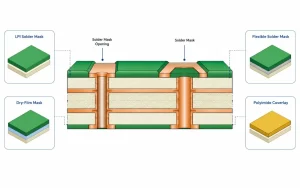
PCB solder mask materials are permanent polymer systems applied over copper to protect the board and control where solder can contact pads. Common options include
PCB solder mask materials are permanent polymer systems applied over copper to protect the board and control where solder can contact pads. Common options include
Customer Success Management A centered customer success management circular diagram recreated with HTML and SVG. Obsolescence Management Design-to-cost Design-to-supply Consulting Engineering Rapid Prototyping Printed Circuit
Choose flying probe testing for prototypes, changing designs, and high-mix builds. Choose in-circuit testing (ICT) when the PCB and BOM are stable and recurring volume
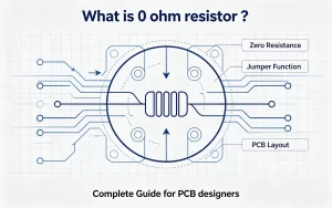
Introduction As a first thought, one might think that the 0 Ohm resistor is unnecessary; after all, why would someone use a resistor with no
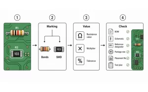
To read a resistor on a PCB, first identify the marking method. Through-hole resistors usually use color bands. SMD resistors usually use numbers, letters, or
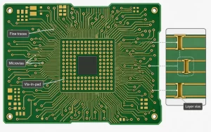
An HDI PCB is a high-density interconnect printed circuit board. It uses finer traces, smaller vias, and denser routing than a standard board. Most designs