Copper Pour in PCB Design: Fill Empty Areas for Better Manufacturing
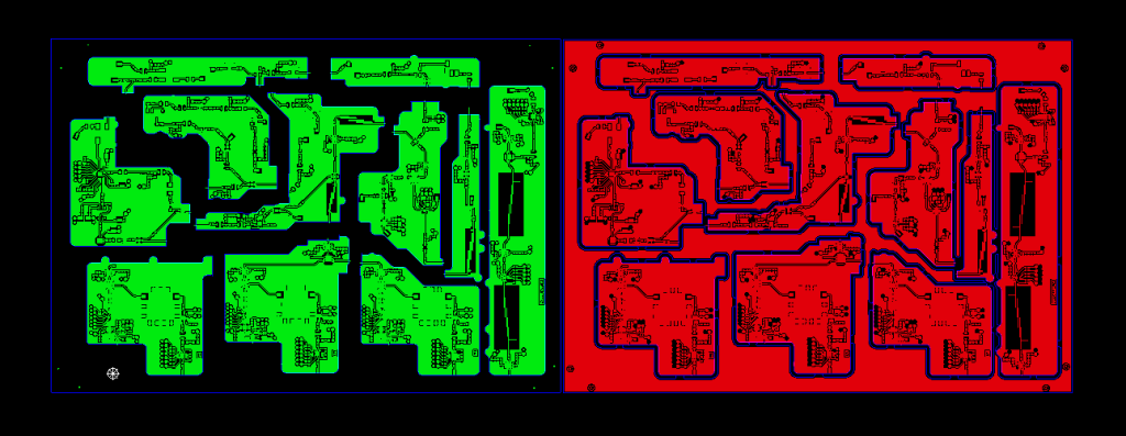
When electronic engineers create printed circuit boards (PCBs), they tend to leave many copper-free areas on the board. They are probably not aware of the technicalities of the PCB production process. A high percentage of the copper-free area on the board can have a negative impact on the product and leave it susceptible to early damage.