Silkscreen PCB is the printed legend layer that helps people read a circuit board during assembly, testing, repair, and traceability work. It is not just decoration. A clear PCB legend can prevent wrong connectors, reversed diodes, hidden test points, and mixed-up board revisions.
PCB silkscreen does not carry current, but it affects how fast a team can build and service the board. Good markings help operators identify parts, confirm polarity, scan traceability codes, and debug hardware without opening the layout file every time.
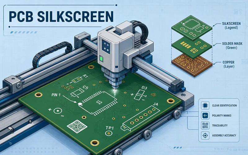
What Is the Silk Screen Layer of a PCB?
The silk screen layer of a PCB is the visible text and symbol layer printed on the board surface. Engineers also call it the PCB legend, legend layer, PCB overlay, or PCB marking layer.
This layer helps operators find components, check orientation, read connectors, identify test points, and confirm the board version. It should support the schematic, BOM, Gerber files, pick-and-place file, and PCB assembly drawing. It should not replace them.

Common PCB Legend Information
- Reference designators such as R1, C5, U2, D3, J4, and TP1.
- Polarity marks for LEDs, diodes, capacitors, and power inputs.
- Connector labels such as USB, UART, CAN, HDMI, GPIO, and DC-IN.
- Pin 1 marks for ICs, connectors, modules, and headers.
- Board revision, serial number, QR code, logo, and warning symbols.
What Is Silkscreen PCB Printing?
Silkscreen PCB printing is the process of adding readable text, symbols, and graphics to a circuit board. The manufacturer applies non-conductive ink on top of the solder mask and cures it for handling, soldering, cleaning, and SMT assembly.
| Printing Method | Best Use | Main Limitation |
|---|---|---|
| Screen printing | Simple boards with open space | Lower precision on small details |
| LPI | Sharper legends and dense layouts | More process setup |
| DLP | High-precision legend output | Higher cost |
| Inkjet printing | QR codes, barcodes, and serial numbers | Needs stable process control |
PCB Silkscreen Material and Ink

PCB silkscreen usually uses non-conductive epoxy ink, acrylic ink, UV-curable ink, or liquid photoimageable ink. The ink must bond well to the solder mask and stay readable after reflow, cleaning, coating, and normal handling.
White silkscreen is common because it gives strong contrast on green, blue, red, and black solder mask. Black silkscreen works better on white solder mask. In production, contrast matters more than brand color.
Conformal coating and PCB potting can reduce label contrast. A QR code may scan well after bare board fabrication but fail after conformal coating or encapsulation. Always check barcode and QR code readability after the final assembly process.
PCB Silkscreen Symbols
PCB silkscreen symbols help teams read the board faster. Common markings include R for resistor, C for capacitor, U for IC, D for diode or LED, J for connector, JP for jumper, and TP for test point.
Polarity marks often matter more than logos. A plus sign, minus sign, diode cathode mark, Pin 1 dot, or connector orientation mark can prevent wrong assembly during prototype builds and rework.
- R marks a resistor.
- C marks a capacitor.
- U marks an IC, MCU, memory chip, or power controller.
- D marks a diode or LED.
- J marks a connector.
- TP marks a test point for ICT, flying probe, or debug.

PCB Silkscreen Design Rules
Good PCB silkscreen starts with readability. Small text may look fine in CAD software but blur, break, or disappear during real production. Review the final Gerber output, not only the layout screen.
Use Practical Text Size
As a common starting point, use at least 0.8 mm to 1.0 mm text height and 0.12 mm to 0.15 mm stroke width. Use larger text when space allows. Always follow your PCB manufacturer’s DFM rules because process limits can vary.
Keep Critical Marks Visible
Place Pin 1 marks, polarity marks, connector names, and test point labels where people can still see them after assembly. A label hidden under a connector, shield, battery holder, display, or heat sink gives no value during inspection or repair.
Checklist Before Sending Gerber Files
- Confirm that reference designators are not hidden under large components.
- Confirm that Pin 1 and polarity marks sit near the correct footprint.
- Confirm that silkscreen does not overlap pads, vias, or exposed copper.
- Confirm that top and bottom silkscreen layers export correctly.
- Confirm that QR codes and barcodes are large enough to scan.
- Confirm that connector labels match the schematic and assembly drawing.
Common PCB Silkscreen Mistakes

- Hidden designators: A label under a relay, shield, display, or connector cannot help the assembly team.
- Polarity marks too far away: A polarity mark should sit close to the diode, LED, capacitor, or power input it controls.
- Wrong connector names: If the PCB says UART1 but the schematic says J3, production teams may need extra confirmation.
- Small QR codes: QR codes can fail after ink spread, soldering, cleaning, or coating.
- Too many labels: Crowded silkscreen can become harder to read than no silkscreen.
- Missing bottom labels: Double-sided boards often need bottom-side labels for test points, jumpers, and revision data.
PCB Silkscreen vs Solder Mask
PCB silkscreen and solder mask are different layers. Silkscreen gives information to people. Solder mask protects copper and helps prevent solder bridges. Copper carries current.
| Item | Main Role | Risk If Poorly Designed |
|---|---|---|
| Silkscreen | Shows labels, marks, and symbols | Assembly, test, or repair confusion |
| Solder mask | Protects copper and controls solder flow | Solder bridges or exposed copper |
| Assembly drawing | Gives controlled build instructions | Wrong build interpretation |
If board space is limited, keep critical marks on the PCB and move secondary notes into the assembly drawing. Do not sacrifice solder mask clearance for decorative text or logos.
How to Silkscreen a PCB

- Place reference designators, connector labels, polarity marks, and test point names in the PCB layout tool.
- Check text size, stroke width, pad clearance, and component visibility.
- Export top and bottom silkscreen Gerber files with the full fabrication package.
- Review the Gerbers against the schematic, BOM, pick-and-place file, and assembly drawing.
- Ask the PCB manufacturer to check dense, coated, or traceability-critical areas.
A broader DFM review can also catch related problems. This list of common PCB DFM mistakes is useful before sending files to fabrication.
When PCB Silkscreen Matters Most
PCB silkscreen matters most during prototype debug, production test, field repair, and long-lifecycle support. Engineers need clear labels for power rails, reset pins, boot jumpers, UART headers, test points, and board revisions.
Industrial, medical, telecom, and automotive boards may need service years after release. Clear revision codes, connector names, and warning marks help technicians identify the right board without relying only on old documents.
Working With a PCB Manufacturer
Silkscreen review should happen before the first panel is built. A useful review checks whether operators can still see the mark after assembly, whether ink will be clipped near pads, whether QR codes will scan after coating, and whether connector names match the files used on the production floor.
For dense SMT boards, coated assemblies, traceability labels, or long-lifecycle products, silkscreen should be reviewed as part of the full DFM package. Weller PCB can support PCB fabrication and assembly projects that need clear legends, reliable documentation, and production-ready review. You can also request an instant quote for PCBA solutions when your design is ready for manufacturing feedback.

Conclusion
PCB silkscreen is a small layer with real production value. It helps teams assemble, inspect, test, trace, and repair boards faster. Keep critical labels clear, close to the right parts, and visible after assembly. Move secondary notes into controlled documents.
FAQ
Is PCB silkscreen conductive?
No. PCB silkscreen normally uses non-conductive ink. It should not carry signals or power.
Can silkscreen be printed over vias?
It should usually stay away from exposed vias. Ink over vias may be clipped, broken, or unreadable.
What file contains PCB silkscreen?
PCB silkscreen is usually included in top and bottom silkscreen Gerber files.
Can QR codes be printed as PCB silkscreen?
Yes. The QR code must be large enough to scan after printing, soldering, cleaning, and coating.
What is the difference between PCB silkscreen and solder mask?
Silkscreen shows labels and symbols. Solder mask protects copper and helps control solder flow.


