Table of Contents

Stripline vs Microstrip: PCB Stackup Selection Guide

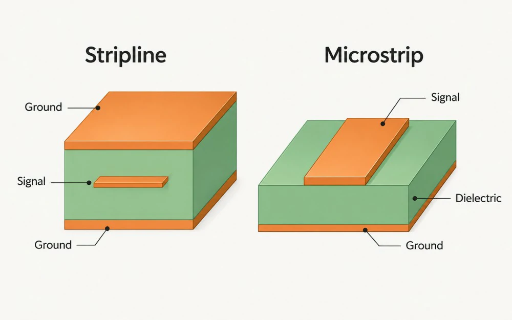
Stripline vs microstrip PCB stackup showing signal and ground layer placement
Neither structure wins every stripline vs microstrip comparison. Microstrip places the signal on an outer layer, which favors direct component launches, probing, and fewer layer transitions. Stripline embeds the signal between reference planes, which generally improves field containment when those references remain continuous.
For a high-speed digital or RF path, start with the intended layer assignment and PCB trace impedance target. Then compare the finished stackup, materials, transitions, frequency or edge-rate range, and validation plan.

How Microstrip and Stripline Differ

The main difference is the transmission-line cross-section. This changes the dielectric environment, reference structure, field distribution, propagation behavior, and connection to surface components.

Microstrip

A PCB microstrip normally runs on an outer copper layer above a reference plane. Part of its field travels through the PCB dielectric and part through the region above the trace, so it is usually modeled as a quasi-TEM structure.
Its direct surface access simplifies component launches, inspection, and probing. However, solder mask, nearby copper, reference discontinuities, and the exposed field must be considered in the impedance and signal-integrity model.

Stripline

Stripline places the signal on an inner layer between reference planes. In contrast to microstrip, an ideal stripline in a homogeneous dielectric is modeled as TEM. The surrounding planes generally provide stronger field containment when the reference structure remains continuous.
Because the signal is internal, surface components and test points normally require vias or other transitions. As a result, those transitions become part of the electrical channel.
Stripline field distribution between two ground planes in PCB dielectric

Microstrip vs Stripline at a Glance
CriterionMicrostripStripline
LocationOuter layerInner layer
ReferenceOne nearby planePlanes above and below
Surface accessDirectVia required
Field containmentMore exposedStronger
PropagationOften fasterOften slower
Main cautionMask and couplingPlane continuity

Propagation delay must be calculated from the actual construction. Common FR-4 transmission lines are often roughly in the 140–180 ps/in range, but this is only an order-of-magnitude reference, not a layout rule.

Choose by the Main Design Constraint

Choose a starting topology from the constraint that matters most, then verify it against the complete channel rather than evaluating only a straight section of trace.

Stripline vs Microstrip Decision Guide

Use the dominant constraint as the starting point.

Constraint Starting Point Check Before Release
Direct launch or probing Microstrip Mask, coupling, reference continuity
Strong field containment Stripline Plane continuity and transitions
Fewer signal vias Often microstrip Launch impedance
Limited layer count Often microstrip Manufacturable spacing
Tight loss budget Calculate both Dk, Df, roughness, geometry, transitions
Controlled impedance Either Stackup and verification method

Do Not Reuse Trace Widths Across Stackups

A width that produces 50 Ω on one PCB may not produce 50 Ω on another because reference spacing, finished copper, dielectric properties, and solder mask can change.
!
  • Recalculate with the production stackup.
  • Do not assume one topology is always lower loss.
  • Include vias, launches, and reference changes.

Microstrip vs Stripline Impedance, Delay, and Loss

Microstrip impedance geometry showing trace width thickness dielectric height and field distribution

Impedance Depends on the Cross-Section

Neither topology has a fixed impedance. Instead, the calculation depends on trace width, finished copper thickness, reference-plane spacing, and dielectric properties. Differential pairs also depend on pair spacing and coupling.

Use the intended production construction for calculation or field solving. Texas Instruments’ High-Speed Layout Guidelines, SCAA082A treats microstrip and stripline as different structures with distinct geometry, dielectric, propagation, and return-path behavior.

Example: Two Paths to a 50 Ω Target

The same impedance does not mean the same geometry.
Input Microstrip Stripline
Target 50 Ω 50 Ω
Signal layer Outer layer such as L1 Internal layer such as L3
Reference Nearby plane Planes above and below
Surface connection Direct Via normally required
Trace width Stackup-specific Stackup-specific
Note: This table does not specify production trace dimensions. Those require the actual dielectric thickness, finished copper, material data, and layer construction.

Propagation Delay Is Layer-Specific

Microstrip effective permittivity showing electric field through air and PCB dielectric

Microstrip often has a lower effective dielectric constant because part of its field travels outside the PCB dielectric. By contrast, stripline keeps more field inside the dielectric and therefore often has greater delay in a comparable material system.

For timing-sensitive channels, calculate propagation for the selected layers rather than assuming identical delay per unit length across the PCB.

Neither Structure Is Automatically Lower Loss

Insertion loss includes conductor loss, dielectric loss, radiation, copper roughness, geometry, and discontinuities. However, their relative importance changes with frequency and construction.
At microwave and millimeter-wave frequencies, Rogers’ PCB design and fabrication guidance shows how material properties, copper roughness, conductor geometry, solder mask, and surface finish can affect insertion loss and phase behavior.
Technical Evidence Reference scope for the key design conclusions.
TI
Transmission-Line Geometry Microstrip, stripline, impedance, propagation, and return paths
Rogers
High-Frequency Loss Factors Material, roughness, geometry, mask, and finish at microwave/mmWave frequencies
Therefore, compare the modeled or measured channel over the required frequency range instead of assigning a universal loss advantage to either topology.

Transitions Can Override the Trace Advantage

Vias, connector launches, stubs, and reference changes introduce discontinuities. For example, an internal stripline may provide good field containment but still perform poorly if its transitions are not designed correctly.
Complete Channel Check
Trace geometry
Via transitions
Connector launches
Reference changes
Return paths
Stub effects

From Stackup Selection to Fabrication

The electrical model should remain tied to a construction that the PCB fabricator can actually produce.

Controlled-Impedance Workflow

  1. Assign the layer. Define the signal and continuous reference structure.
  2. Next, calculate the geometry. Use the proposed materials and finished construction.
  3. Manufacturability review comes next. Confirm copper, dielectric thickness, materials, and trace limits with the fabricator.
  4. Finally, define verification. Agree on calculation, TDR, or an impedance coupon before fabrication.
Fabrication Input Template

Provide these inputs before controlled-impedance fabrication.

Impedance Target and tolerance
Signal Context Interface and frequency / edge rate
Layer / Reference Signal layer and reference plane
Stackup Materials and dielectric spacing
Copper / Geometry Finished copper, width, pair spacing
Transitions Vias, connectors, launches
Loss Details Roughness, mask, surface finish
Verification Calculation, coupon, or TDR

A Practical Stripline-or-Microstrip Decision

Use microstrip when direct surface access, simple launches, probing, or fewer layer transitions dominate. Use stripline when field containment between continuous reference planes is more important.
For tight impedance, insertion-loss, or transition requirements, evaluate both structures using the production stackup and complete channel rather than making the choice from topology alone.
For stackup, layer-assignment, and controlled-impedance review, provide the channel requirements when requesting a PCB layout quote from WellerPCB.

Stripline vs Microstrip FAQ

Is stripline always lower loss than microstrip

No. Loss depends on material properties, copper roughness, geometry, frequency, length, and discontinuities. Evaluate the complete channel using the intended production stackup.

Stripline generally provides stronger field containment when continuous reference planes surround the trace. Poor transitions, plane breaks, and connectors can still create radiation and coupling.

Not generally. Both require stackup-specific impedance calculations based on finished copper, dielectric spacing, material properties, and, for differential pairs, conductor spacing.

Compare signal rise or fall time with interconnect delay and electrical length. Clock frequency alone is not sufficient because relatively low-frequency signals can still contain very fast edges.
Provide the impedance target and tolerance, layer and reference assignment, stackup, materials, finished copper, trace geometry, frequency or edge-rate context, major transitions, and required verification method.

SHARE POST

By Kevin

I have over 10 years of experience in PCB manufacturing. My work includes PCB fabrication, SMT assembly, DFM review, supplier communication, and electronics production support. In my writing, I explain PCB design, layer stack-up, assembly processes, quality control, and production planning in a practical way. My goal is to help readers make better manufacturing decisions.

Recent Posts

Get In Touch With Us Today

Drag & Drop Files Here (dsn, pdf, xlsx, dxf, zip, rar up to 8M)
or
This form is protected by Google’s Terms of Service and Privacy Policy.

Related Posts

Eye diagram analysis interface showing jitter, eye height, eye width, and voltage distribution

An eye diagram overlays repeated digital transitions to show voltage and timing margin.

IPC J-STD-001 requirements for controlled PCB assembly quality and workmanship

IPC J-STD-001 defines material, process, inspection, and acceptance requirements for soldered electrical and.

Leave a Reply

Your email address will not be published. Required fields are marked *