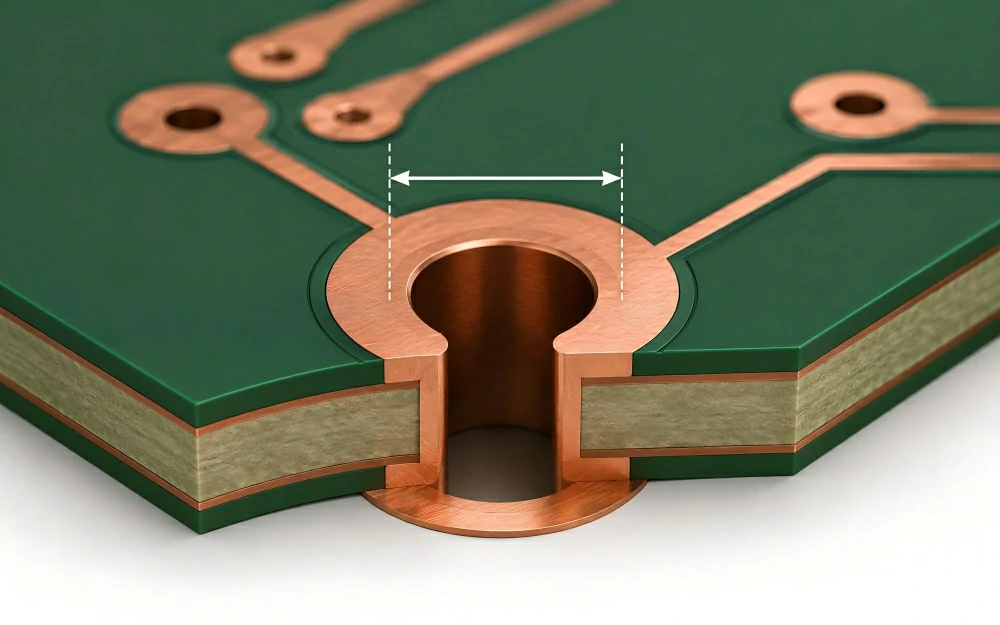
A PCB annular ring is the copper land between a drilled hole and the outer edge of its pad. For a centered circular pad and hole, the nominal radial width equals (pad diameter – hole diameter) / 2. This value describes ideal CAD geometry, not the minimum copper guaranteed on a finished board.
What Is a PCB Annular Ring?

A PCB annular ring belongs to the copper pad, or land, surrounding a drilled hole. It may support a plated component hole, through via, blind via, buried via, or another drilled structure. Ring width is measured radially, while pad and hole dimensions are usually specified as diameters.
Confirm Which Hole Diameter the Calculation Uses
A drill-tool diameter, drilled-hole diameter, and finished-hole diameter can describe different stages of PCB fabrication. Do not treat them as interchangeable inputs.
How to Calculate Nominal and Minimum Ring Width

The nominal calculation assumes perfect alignment. When the hole center shifts relative to the pad center, one side gains copper while the opposite side loses the same radial amount. A simplified one-layer estimate is:
Predicted minimum ring = nominal annular ring – center offset
Nominal and Predicted Minimum Annular Ring
This example shows how a centered 0.20 mm nominal ring is reduced when the hole center shifts by 0.10 mm.
| Input | Example Value | Engineering Purpose |
|---|---|---|
| Pad diameter | 0.80 mm | Defines the available copper land. |
| Hole diameter | 0.40 mm | Defines the opening evaluated in the calculation. |
| Nominal ring | 0.20 mm | Represents the ideal centered radial width. |
| Center offset | 0.10 mm | Represents positional displacement on the evaluated layer. |
| Predicted minimum ring | 0.10 mm | Estimates the remaining copper at the narrowest location. |

In this simplified geometry, a 0.20 mm offset produces tangency because the narrowest ring reaches zero. An offset greater than 0.20 mm produces breakout. Actual finished-board acceptance still depends on the affected layer, connection, product requirements, and agreed inspection criteria.
Tangency and Breakout Conditions

Classify the Narrowest Annular Ring Condition
Evaluate the remaining copper at the narrowest point, then determine whether the feature can proceed, needs review, or must be redesigned.
Does copper remain continuously around the complete hole circumference on the evaluated layer?
Contained Annular Ring
Tangency
Breakout
- The affected outer or inner layer
- Whether the land is functional or nonfunctional
- Trace-entry and plane-connection direction
- Hole type and finished-hole definition
- Product class and procurement requirements
- Applicable inspection and acceptance criteria
How to Size a Pad from the Finished Requirement
Size the Pad from the Required Finished Ring
Start with the required remaining copper, then add the evaluated hole size and manufacturing offset allowance.
Minimum pad diameter = maximum hole diameter + 2 × (required finished ring + manufacturing offset allowance)
0.40 + 2 × (0.10 + 0.08) = 0.76 mm
Design Rules, Fabricator Capability, and IPC Documents
An annular-ring number can describe a CAD rule, supplier capability, or finished-board acceptance criterion. These values are related but not interchangeable.
Do Not Treat Every Annular-Ring Value as the Same Requirement
Identify whether a value controls layout geometry, manufacturing capability, or finished-board acceptance before applying it.
CAD Design Rule
Fabricator Capability
Finished Acceptance Criterion
The project must still define the selected performance class, board construction, procurement requirements, customer deviations, and inspection basis. Do not copy one public “minimum annular ring” value into every design without confirming its scope.

How to Prevent Annular Ring Breakout
| Finding | Preferred Action | Verify Before Release |
|---|---|---|
| Pad is too small | Increase the pad diameter | Copper spacing and routing clearance |
| Hole is larger than necessary | Review the finished-hole requirement | Lead size, fit, and assembly allowance |
| Registration margin is uncertain | Obtain construction-specific capability data | Layer count, materials, hole type, and process |
| Inner-layer land is constrained | Adjust the land or connection geometry | Plane clearance and trace-entry direction |
| Via density prevents a larger pad | Review the routing or use another via structure | Cost, reliability, and supplier capability |
| CAD and drawing values conflict | Reconcile the drill and fabrication data | Tool size versus finished-hole size |
Pre-Fabrication Annular Ring Checklist
Annular Ring Release Checklist
Complete these checks before releasing the PCB fabrication package.
-
1
Classify the hole Separate component holes, ordinary vias, and special via structures.
-
2
Confirm the dimension basis Identify the drill-tool, drilled-hole, and finished-hole values.
-
3
Review every relevant layer Check outer and inner lands, plane connections, and trace-entry directions.
-
4
Run the CAD DRC Investigate exceptions instead of disabling the rule globally.
-
5
Apply actual capability data Use allowances for the selected stack-up, materials, and drilling process.
-
6
Reconcile all outputs Compare copper data, drill data, drawings, tolerances, and fabrication notes.
-
7
Record governing requirements State the applicable design, performance, and acceptance documents.
-
8
Escalate tight locations Request fabricator review before freezing the fabrication package.
Design from the Finished Annular Ring Backward
Design from the Required Finished Annular Ring
Start with the finished-board requirement, add documented process allowances, and verify the resulting geometry before release.
PCB Annular Ring FAQs
What Is the Difference Between Nominal and Finished Annular Ring?
What Causes Annular Ring Breakout?
Is Tangency the Same as Breakout?
No. Tangency occurs when the hole edge reaches the pad boundary at one point. Breakout occurs when the edge crosses the boundary. Both conditions require review of the layer function, connected geometry, and governing requirements.