Introduction
Before talking about In-Circuit Testing for printed circuit boards. Do you ever wonder how electronic manufacturers use different types of methods to confirm that the printed circuit boards operate correctly prior to delivery at the customer level? Modern electronic devices are rapidly increasing in size and complexity. A minor PCB defect can create a failure of the product which can result in customer dissatisfaction. This is where in-circuit testing (ICT) becomes vital. ICT provides manufacturers the ability to test each component and circuit connection on the PCB while still in its assembled state.
The use of this technology allows the manufacturer to find defects earlier in the manufacturing process and to produce higher-quality products consistently. This article covers in-circuit testing, how it works, the benefits of ICT, common defect detection methods with ICT, and the importance of ICT in today’s PCB manufacturing environment.
What is In-Circuit Testing?
In-Circuit Testing (ICT) is an electrical test technique in which circuit boards are tested individually using an automated tester. This process allows for verification of the function and integrity of individual components on a printed circuit board assembly (PCBA) and interconnections between them through the use of specialized probes connected to designated test points on the PCB.

While measuring the parameters like resistance, capacitance, inductance, voltage, and continuity utilised during testing through connections between the components, ICT will also detect the orientation of the components on the PCBA. Unlike a functional test, which provides testing results for the entire board, ICT tests the components manufactured for defects at the time of manufacturing. Due to the speed, accuracy, and repeatability of ICT, this testing technique is frequently used as a form of quality assurance in the high-volume production of electronic products.
How In-Circuit Testing Works?
Controlled electrical stimuli, like voltage and current, can be applied to individual nodes on the PCB in order to produce a response and record the response. The operation of ICT will be controlled by a pre-programmed test script(s), and it also uses special hardware to accomplish these tasks.
Step 1: Designing the Bed-of-Nails Fixture
For each specific PCB design, a unique fixture containing a number of spring-loaded probes is designed and manufactured. These probes must be placed so that they can make contact with specific test points on the PCB. During the execution of ICT, all probes will simultaneously make contact with their respective test node when the PCB is properly positioned into the fixture.
Step 2: Creating the Test Program
Using a variety of ICT software tools, which are developed by Keysight test engineers to enhance the test program. The test program will specify which nodes will be probed, what stimuli will be delivered, and what measurement ranges can be expected for each component.
Step 3: Probing & Board Loading
After the PCB has been manufactured, it is placed into the fixture and secured. The fixture then uses either a mechanical or pneumatic actuator to press the PCB down so that all probes make a solid connection simultaneously. The ICT system will then execute the test program in the order they were created.
Step 4: Electrical Measurement
Electrical Measurement is an essential aspect of digital testing. The ICT system measures and applies signals to many electrical parameters, such as Resistance, Capacitance, Inductance, Voltage, Frequency, and Current. Boundary scan or JTAG techniques test internal logic on a digital IC without having to physically access every pin.
Step 5: Pass or Fail Determination
Pass or fail determination is done by comparing the expected values to the measured values in the test program. If the measured value deviates from the expected tolerance window, the system marks that component as a failure. Depending on the seriousness of the failure, the Board of PCBs is routed for either scrap or rework.
Step 6: Data Logging and Analysis
All test results are recorded in a database for process monitoring. Manufacturing Engineers can use statistical analysis of ICT data to identify recurring process problems and improve soldering and placement procedures over time.
Common Defects Detected by ICT
In-circuit testing (ICT) is used to discover defects that may interfere with PCB operation, performance, and reliability before an assembled PCB board is shipped from the manufacturer.
Open Circuits
If traces are broken or damaged, or if solder joints have not formed properly between adjacent surfaces and conductive paths, there will be an open circuit. The goal of using ICT is to check continuity between test points and locate the open circuits that may be interfering with the transmission of signals or power through a circuit.
Short Circuits
Short circuits are the result of conducting unintended electricity between various conductors. The causes of this problem could include conductive materials like dirt on the PCB, solder bridges or errors made during assembly. ICT is able to identify short circuits by measuring the resistance between adjacent net connections and alerts the manufacturer to the potential for excessive current flow, overheating, and catastrophic failure when the product is operational.
Poor Bending Quality
Solder joint defects can create high resistance, intermittent connections or total circuit failure. ICT assists in the identification of weak electrical connections, cold solder joints and not enough solder being applied. By detecting defects earlier in the production process, the occurrence of costly warranty claims and end-user failures can be reduced while improving the overall quality of the finished product.
ICT Verifies Missing Components
When assembly is performed using machinery, it is possible for parts not to be placed on the PCB. ICT verifies that a part has been placed on the PCB by measuring electrical characteristics at test points and checking the presence of resistors, capacitors, diodes, and integrated circuits.
ICT Test Detects Reversed or Misaligned Polarities
Electrolytic Capacitors, diodes, LEDs and Integrated Circuits are examples of polarised-type components and must be installed in accordance with their polarity markings. ICT enables the detection of reversed or misaligned polarities of these components, thus helping to eliminate the board malfunction or component damage during operation of the completed product.
Types of In-Circuit Testing Systems
Employing different types of ICT (In-Circuit Testing) solutions can help preserve high defect detection capability while allowing for different levels of production volume, board complexity, testing needs and costs associated with production.
Manufacturing Defect Analyser (MDA)
MDA’s (Manufacturing Defect Analysers) can help in evaluating assemblies for assembly defects such as shorts, opens, improper placement of components or missing components, and polarity. MDAs are typically performed using non-powered testing and provide a cost-effective way to identify common faults prior to conducting functional tests on production units.
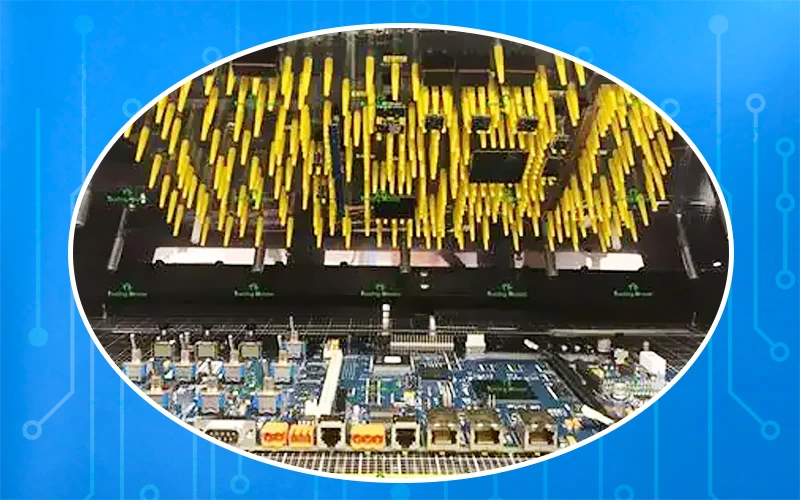
Bed-of-Nails ICT
A Bed-of-Nails system is a specialised test fixture that will provide simultaneous contact to hundreds or thousands of test locations on a PCB via multiple spring-loaded probes, which are also known as “test pins”. This method will allow for high-quality testing speeds and excellent coverage rates in large volume manufacturing, with continuous throughput and repeatability.

Flying Probe Testing
Flying Probes utilises movable probe test heads that are controlled by precision automation and are not reliant upon using specialised fixtures. For testing, the probe access test points on the PCB, testing each target point sequentially. While Flying Probes provide a greater amount of flexibility than Bed-of-Nails test fixtures, they do not provide the same level of efficiency and speed. However, they will provide a way to reduce setup time when working with prototypes and low-volume production.

Why In-Circuit Testing is Important for PCB Quality?
Incorporating In-Circuit Testing (ICT) into the quality control process is vital for manufacturers to identify defects prior to continuing production that eventually enhance manufacturing productivity and ensures that PCBs deliver reliable performance throughout the lifecycle of a product.
Early Defect Detection
ICT allows manufacturers to detect defects in assembled circuit boards immediately upon completion of manufacturing. This prevents defective circuit boards from advancing through the manufacturing process. By identifying defects early in production, manufacturers are able to prevent defective products from reaching consumers, which minimises material waste and reduces repair costs.
Developed Product Reliability
Properly manufactured PCBs play a key role in the reliability of electronic equipment. By ensuring that electrical connections and components function correctly, ICT helps identify hidden manufacturing defects before products reach customers. This improves product reliability and supports consistent performance throughout the product’s lifecycle.
Yield Improvement
The process of detecting and correcting defects early contributes to improved overall manufacturing yield. Manufacturers can also benefit from improved manufacturing results and better utilisation of resources. They do it by identifying and addressing recurring process issues, optimising assembly processes and enhancing the reduction of rejected or reworked boards.
Reduced Troubleshooting Time
ICT provides manufacturers with detailed diagnostic data that allows them to identify the exact location of any defects discovered. By being able to quickly troubleshoot and repair defects, technicians can ensure efficient production operations and resolve defects promptly.
ICT Test Minimising Warranty Costs
Defective products, delivered to customers, can lead to warranty claims, product refunds and product replacement. ICT minimises those risks and protects manufacturers from loss of profits and damage to their brand reputation by providing the capability to find and repair production errors before shipment.
Supports Mass Production
Modern devices need rapid, reliable testing processes to support production. ICT allows the rapid, automated inspection of large manufacturing batches to ensure that quality standards are maintained without impacting production throughput.
Enhancing Client Satisfaction
Consistent quality between products is a major factor influencing customer satisfaction and trust. ICT helps manufacturers deliver reliable electronics that meet or exceed customers’ expectations while reducing in-field failures and increasing product reliability.
Design for Testability (DFT) for ICT
The PCB design process consists of the groundwork for successful in-circuit testing. Boards designed with accessible test points, proper component spacing, and adequate probe access will allow for reliable testing if DFT or Design for Testability principles are applied. Test pads should be positioned appropriately so that the number of inaccessible nodes is minimised, which should create adequate space around components. ICT fixture specifications must be followed, and the integration of DFT principles early on will provide greater test coverage, reduced fixture complexity, and improved defect identification. A good design can help manufacturers increase the effectiveness of ICT and reduce costs associated with testing and production delays.
ICT vs Other PCB Testing Methods
Different PCB testing methods serve distinct purposes throughout the manufacturing process.
Testing Method
Primary Purpose
Defects Detected
Speed
Coverage
In-Circuit Testing (ICT)
Component-level electrical verification
Shorts, opens, missing parts, wrong values
Very Fast
High
Flying Probe Testing
Electrical verification without fixtures
Similar to ICT
Moderate
High
Functional Testing (FCT)
Verifies overall board operation
Functional failures
Moderate
Medium
Automated Optical Inspection (AOI)
Visual inspection of assembly quality
Solder defects, placement errors
Fast
Visual Only
X-Ray Inspection
Internal structure analysis
Hidden solder joint defects
Moderate
Specialized
Boundary Scan Testing
Digital circuit verification
Connectivity faults
Fast
Limited to supported devices
ICT, FCT and EOL testing processes, what is the Relationship between them?
Here is the process flow diagram:
SMT Soldering → 🎯 ICT → Firmware Programming → 🎯 FCT → Full Product Assembly → 🎯 EOL → Shipment
Category
Powered On?
Testing Focus
Equipment
In-Circuit Testing (ICT)
❌ No power supply
Component-level inspection & circuit integrity
ICT tester, probe fixture
Flying Probe Testing
✅ Powered on
Functional logic & software operation
Test fixture + industrial control computer
EOL (End Of Life)
✅ Powered on
Complete machine performance & user experience
Vehicle interface simulation equipment
Challenges of In-Circuit Testing
Despite ICT being highly effective and functional, there are several challenges for manufacturers needing to be overcome to get the maximum test performance.
- The bed of nails tester needs a specific type of fixture to operate.
The cost of making fixtures and maintenance is very high. - Due to the high density of components placed on a PCB, there is limited access to test points.
- As component sizes and density continue to get smaller, there will be fewer available test points.
- Not all electrical failures can be detected functionally.
- Specific knowledge is needed for developing test programs.
- Due to inherent changes to designs, modifications to fixtures will be required on a regular basis.
Conclusion
To ensure quality PCB manufacturing, the most important test methodology still used today is in-circuit test or “ICT.” Manufacturers are able to boost production yields, cut down on costs and create dependable electronic devices through the early identification of manufacturing defects, such as shorts, open circuit traces, missing components, misplaced value parts, or issues with soldering, by utilising an effective ICT strategy. ICT strategies together with testability through design (DFT) principles are becoming incredibly important as PCB design continues to evolve to be more complex.
Weller PCB utilizes extensive in-circuit testing in manufacturing process will help you to reduce manufacturing errors and improve overall PCB quality. It provides a proven way to achieve higher product quality and improve customer satisfaction.
FAQ
1. How do vintage-style PCB testers compare to modern ones in terms of their design characteristics and usability?
The key difference is that modern ones feature a greater number of layers, smaller components, finer-pitch connectors, and a more compact overall package than older-style testers. Because of these factors, modern printed circuit boards typically have less space available for specific test points. As a result, probe accessibility on modern boards has also been limited, which can lead to reduced test coverage and increased difficulty of developing fixture designs. To continue achieving optimal performance for their in-circuit testing (ICT) systems, as the size of their products decreases, manufacturers will need to utilise more advanced design-for-testability techniques.
2. Is there any flexibility regarding the use of ICT fixtures with different types of PCB designs?
Generally, yes. Typically, a dedicated custom fixture must be built to accommodate the specific layout for a given PCB design along with the associated location of the test points and the associated location of the components. In addition, if the PCB design changes significantly, the fixture must be modified to a new fixture for the new design. Conversely, most flying probe systems can test multiple designs using the same test fixtures, since they do not require custom fixture designs.
3. Why do some manufacturers skip ICT and only use FCT?
Some manufacturers opt to only use Functional Circuit Testing (FCT) because the cost and timeline associated with creating the necessary fixtures for In-Circuit Testing (ICT) can be prohibitive for low-volume production runs. Functional testing verifies whether the assembled PCB performs its intended function under operating conditions. However, FCT may not be able to detect manufacturing defects at the component level . This can result in additional debug time due to insufficient detection of manufacturing defects through FCT alone.
4. Is ICT suitable for low-volume or prototype production?
When implementing prototype builds or low-volume production runs, ICT may be a less cost-effective method because of the expense associated with developing the required ICT test fixtures. In low-volume production or prototyping, manufacturers utilise flying probe testing to perform equivalent electrical verification without requiring the same custom-designed test fixtures. This method allows for faster iterations to the design of a prototype, reduced programming costs, and greater flexibility to make design changes during production.


