Introduction
Modern electronic devices are seamlessly integrated into our daily lives. Technology is transforming everything, shifting how we communicate, work, and access care. The tool that makes sure all this happens is the Printed Circuit Board (PCB). PCB is the foundation of every modern electronic product, from simple embedded devices to complex industrial systems.
But before we manufacture a PCB, we need to design the product schematics and board design layout. Therefore, designing PCB schematics acts as the blueprint of the circuit, showing how components are electrically connected and how the system is intended to function.
This tutorial will help you with the complete process of how to draw a PCB schematic, starting from the understanding of fundamentals to preparing a design that is ready for PCB layout, manufacturing, and PCB assembly.
What is a PCB Schematics?
A PCB schematic is a graphical representation of an electronic circuit that shows how different components are electrically connected to each other. The PCB schematics consist of components such as resistors, capacitors, ICs, sensors, and connectors. These components are represented using the standardized symbols to distinguish between different components and their interconnection.
The components are connected using wires known as nets. This allows designers to define how signals and power flow through the system without actual footprint and physical placement constraints. Modern PCB schematics are designed using various software tools, which include EasyEDA, KiCAD, Altium Designer, and Eagle Designer. These tools help engineers create accurate circuit PCB schematics, manage component libraries, and generate netlists that are later used for PCB layout design.
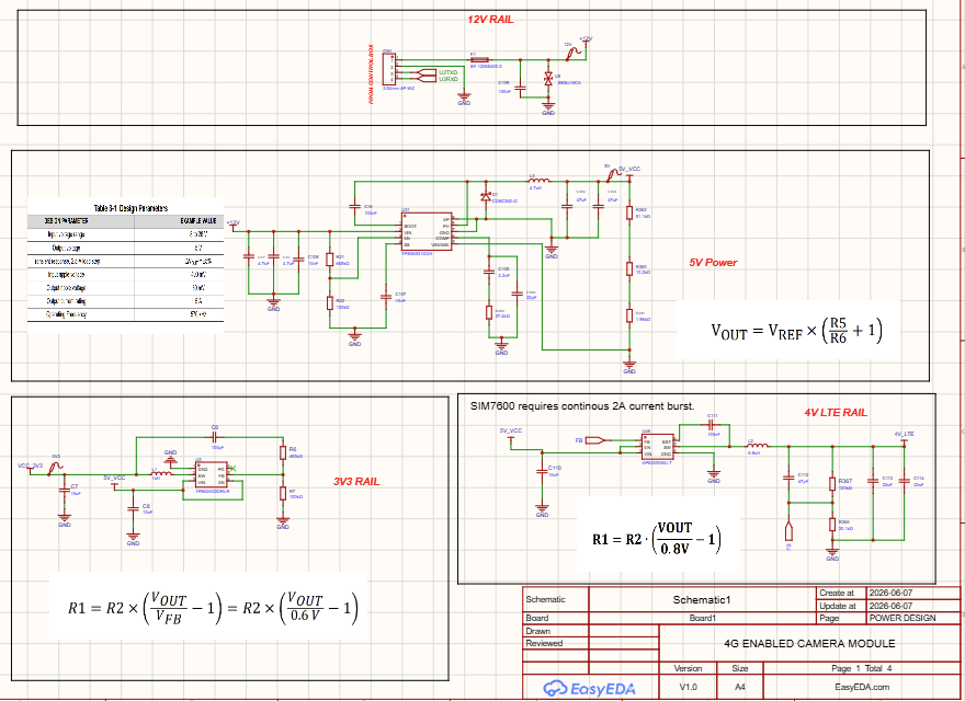
A simple representation of PCB schematics designed in EasyEDA is shown below.
Understanding the PCB Design Workflow
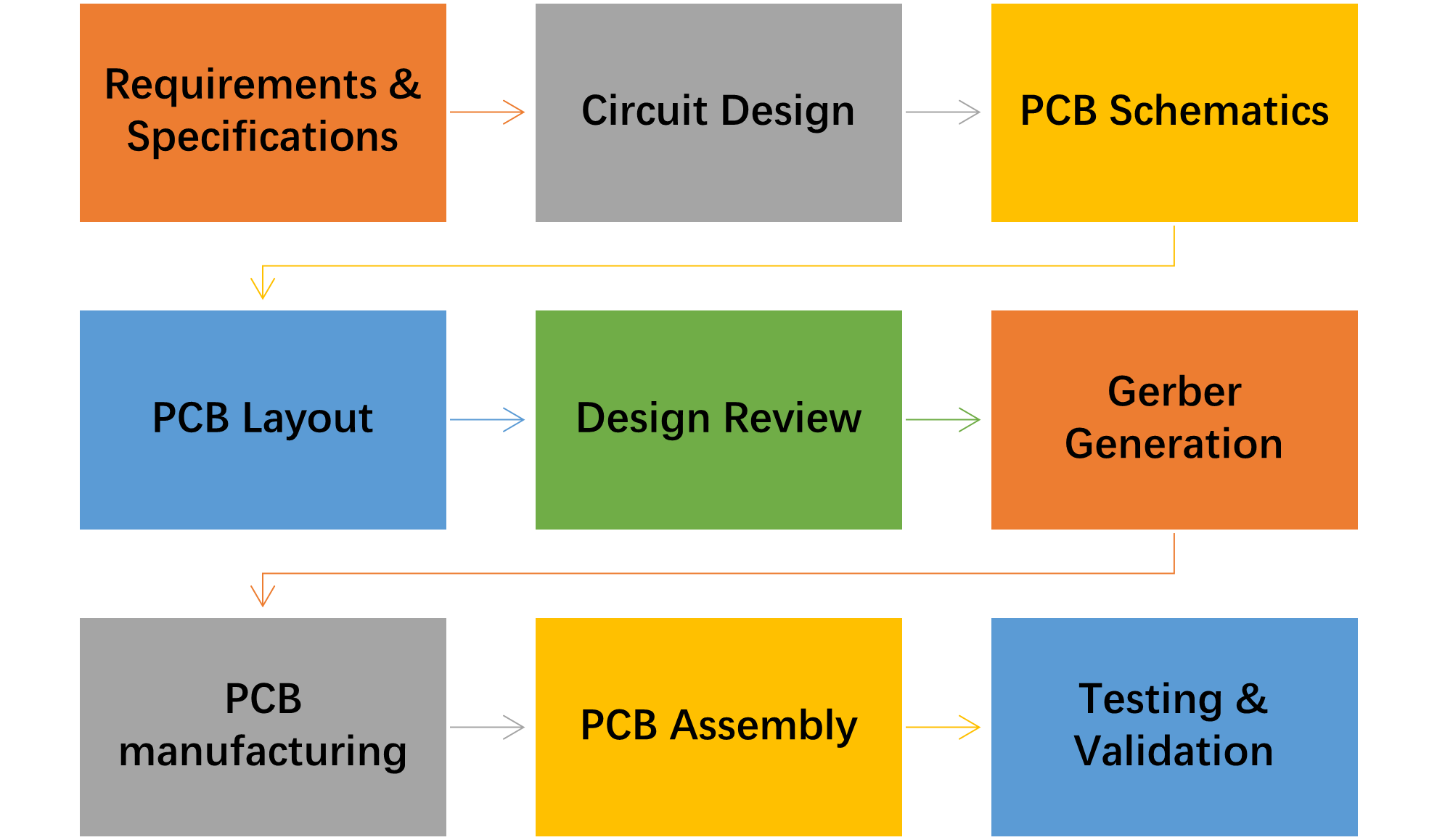
Before we start drawing the PCB schematics, it is far more important that we first understand the general workflow of PCB design. Modern PCB development follows a structured workflow that transforms an idea or product requirement into a fully assembled and tested electronic device. Each stage of the process builds upon the previous one, making it essential to follow a systematic design approach to avoid costly errors and redesigns.
A typical PCB design workflow consists of understanding the specifications, circuit design, PCB schematic, PCB layout, PCB manufacturing, assembly, and testing. Understanding this workflow helps engineers create designs that are not only electrically functional but also manufacturable, reliable, and cost-effective.
1. Requirements & Specifications
- Input and output voltages
- Power consumption
- Communication interfaces
- Environmental conditions
- Size constraints
- Regulatory requirements
- Manufacturing budget
2. Circuit Design
- Select components
- Design power supplies
- Create signal circuits
- Define interfaces
- Perform calculations & simulations
3. Schematic Capture
- Place components
- Create electrical connections
- Define power & ground nets
- Assign values
- Add design documentation
4. PCB Layout Design
- Define board dimensions
- Place components
- Route traces
- Create power planes
- Manage thermal performance
- Apply design rules
5. PCB Manufacturing
- Generate Gerber files
- Create drill files
- Prepare fabrication drawings
- Provide stack-up details
6. PCB Assembly
- Solder paste application
- Pick-and-place assembly
- Reflow soldering
- Through-hole assembly
- Visual inspection
7. Testing & Validation
- Functional testing
- In-circuit testing (ICT)
- Power-up verification
- Signal integrity analysis
- Environmental testing
Information Required Before Drawing a PCB Schematic
Most engineers begin by placing components and connecting wires in the schematics editor, without gathering all the required information.
Generally, for the PCB schematics, there are three major requirements that the designer must know before starting to design schematics, i.e., functional requirements, electrical requirements, and mechanical requirements.
Functional Requirements
The functional requirements consist of knowing the answers of following questions.
1. What is the primary function of the device?
2. What inputs and outputs are required?
3. Which communication interfaces will be used?
4. What processing or control functions are needed?
5. Are there any performance requirements?
Electrical Requirements
Similarly, the electrical requirements form the foundation of component selection and circuit design. The core electrical requirements that the designer must know are input voltage range, output voltage requirements and current consumption, power and protection requirements.
Mechanical Requirements
The mechanical Requirements of the product must be considered before schematic design begins, which includes PCB dimensions, enclosure limitations, connector locations, mounting hole positions, component height restrictions, and thermal management requirements.
Choosing PCB Schematic Design Software
Once you understand the PCB project requirements, scope, workflow, and all electrical and mechanical constraints. It is the right time to select the PCB schematic design software. There are various software tools available, such as KiCAD, EasyEDA, and Altium Designer. However, the choice of software tool often depends on project complexity, budget, and manufacturing goals.

Professional PCB schematics and design layout tools provide improved schematic and design layout, reduce errors, and streamline the overall development workflow from concept to production.
- Advanced schematic capture
- Integrated PCB layout
- 3D PCB visualization
- Design Rule Checking (DRC)
- Extensive libraries
- Industry standard
- Excellent layout tools
- Strong library management
Commercial Products
Complex PCB Designs
- Professional schematic design
- Circuit simulation
- PCB layout integration
- Signal integrity analysis
- Powerful simulation
- Ideal for complex systems
- Enterprise-grade platform
High-Speed Designs
Industrial Electronics
- Schematic capture
- PCB layout
- 3D viewer
- Custom libraries
- DRC support
- Free and open-source
- No design limits
- Strong community support
Students
Startups
Hobbyists
- Cloud-based platform
- Integrated libraries
- Direct PCB ordering
- Collaboration tools
- Easy to learn
- No installation required
- Fast prototyping workflow
Rapid Prototyping
Education
Beginners
- Schematic capture
- PCB layout design
- Library management
- Design Rule Checking
- User-friendly interface
- Large community
- Extensive tutorials
Makers
Small Development Teams
Prototype Designs
Comparison of Popular PCB Design Software
| Software | Cost | Difficulty Level | Best For |
|---|---|---|---|
| Altium Designer | High | Advanced | Professional PCB design |
| Cadence OrCAD | High | Advanced | Enterprise and high-speed designs |
| KiCad | Free | Moderate | Students, startups, professionals |
| EasyEDA | Free / Low Cost | Beginner-Friendly | Rapid prototyping |
| Autodesk Eagle | Moderate | Moderate | Small to medium projects |
Creating a New PCB Schematic Project
Creating a new PCB schematic project is the first practical step in turning an idea into a structured electronic design. Most PCB design tools, such as Altium Designer, KiCad, EasyEDA, and Cadence OrCAD, follow a similar project creation workflow. In this section, I will guide you on how to create a PCB schematic project in EasyEDA, KiCAD, and Altium Designer.
How to Create a PCB Schematic Project in EasyEDA
To begin, open the EasyEDA platform in your browser and sign in to your account.
- You can use Google login or create a separate account
- After login, you will access the EasyEDA design workspace
A registered account allows you to save projects and access cloud storage for your designs.
Once inside the dashboard, click on “File->New->Project” as shown in the figure below.
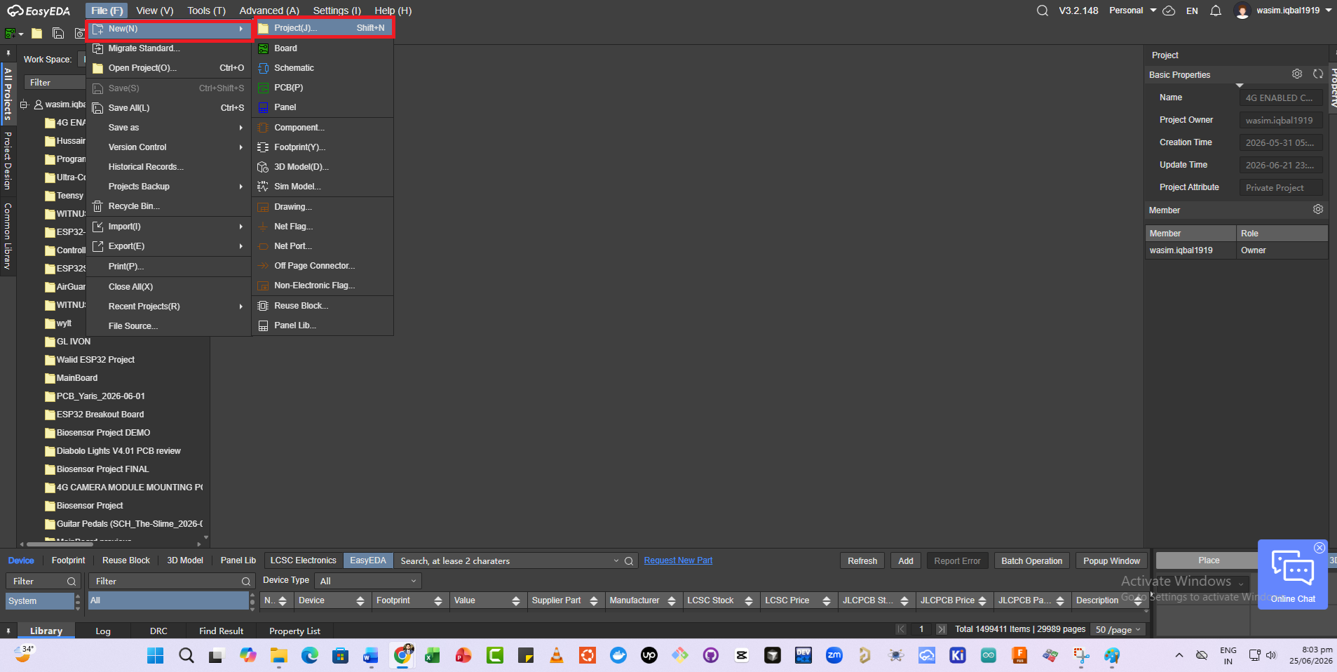
Now, enter the name of your project and click on save as shown in figure below.
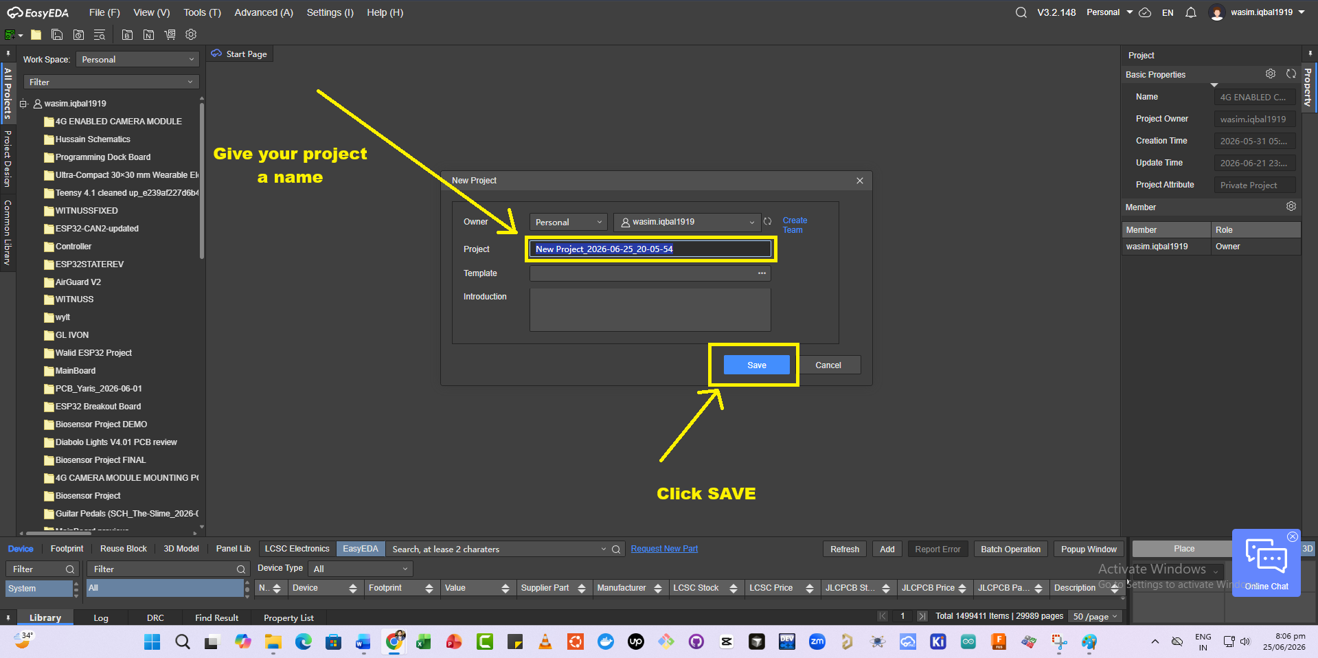
After creating the project, EasyEDA automatically generates a linked schematic and PCB file structure. Now, open the schematic file inside the project.
Changing Schematics Sheet Size
The schematic editor workspace will appear, and you will see a blank canvas for schematic design. This is where you will build your circuit using components and connections.
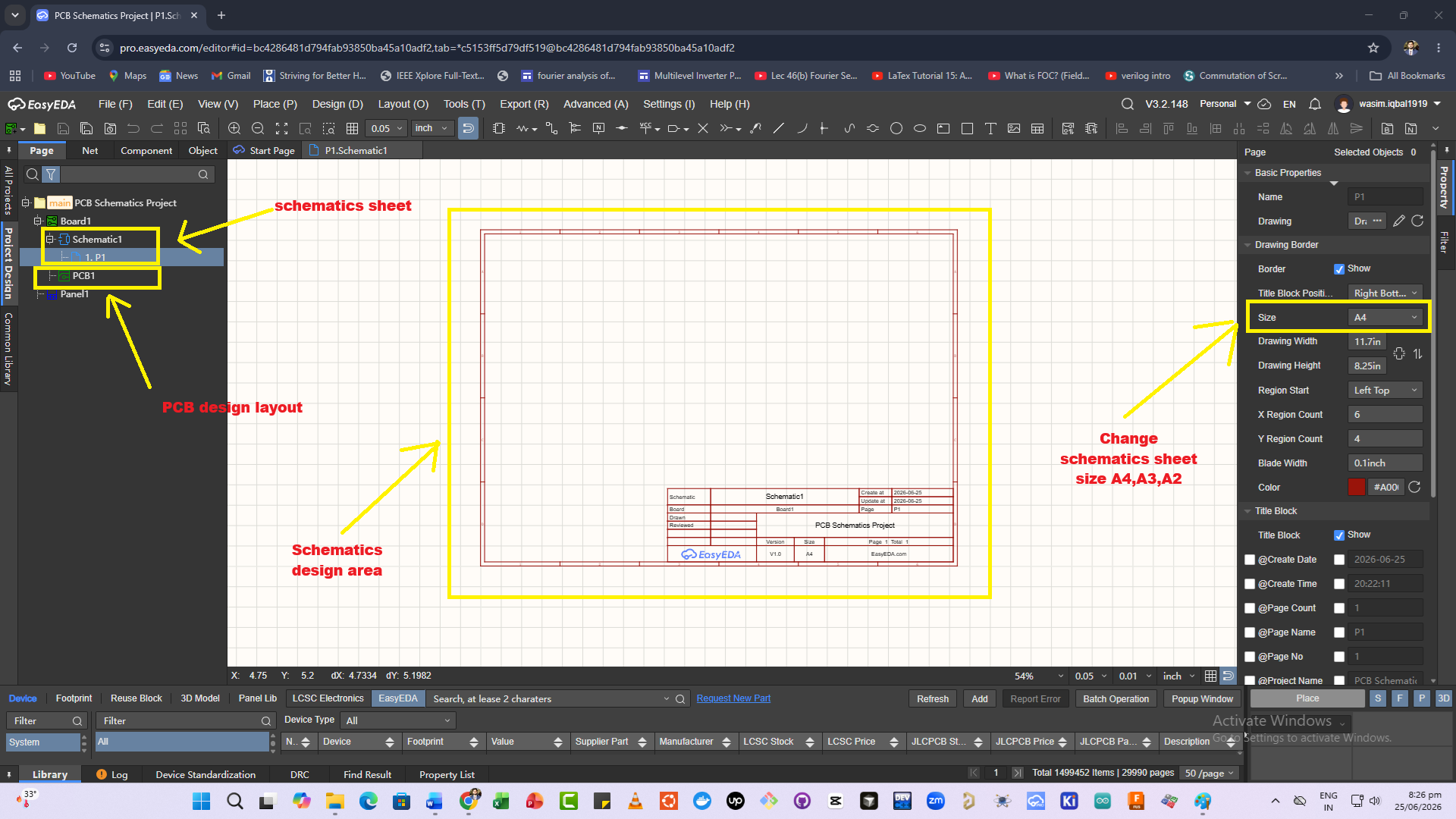
In the schematic editor, you can add multiple schematic sheets, change the grid size, and change the schematic sheet size to A4, A3, or A2 as per your requirements.
Adding Components from Library
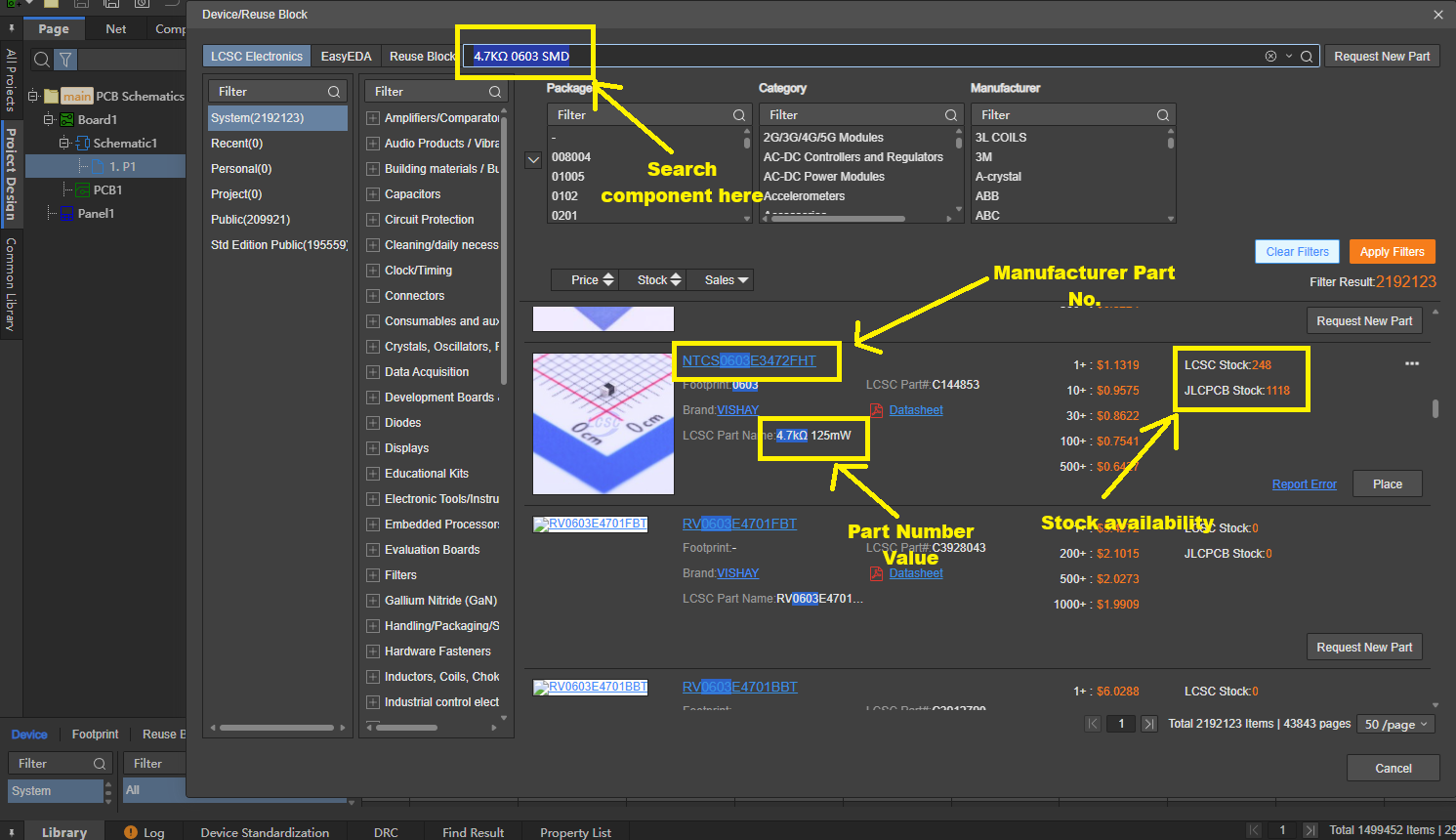
Now, you can add the components from the library. To add components, click on “Libraries” and search for the required components. Now click and place components onto the schematic sheet.
Switching to Design Layout
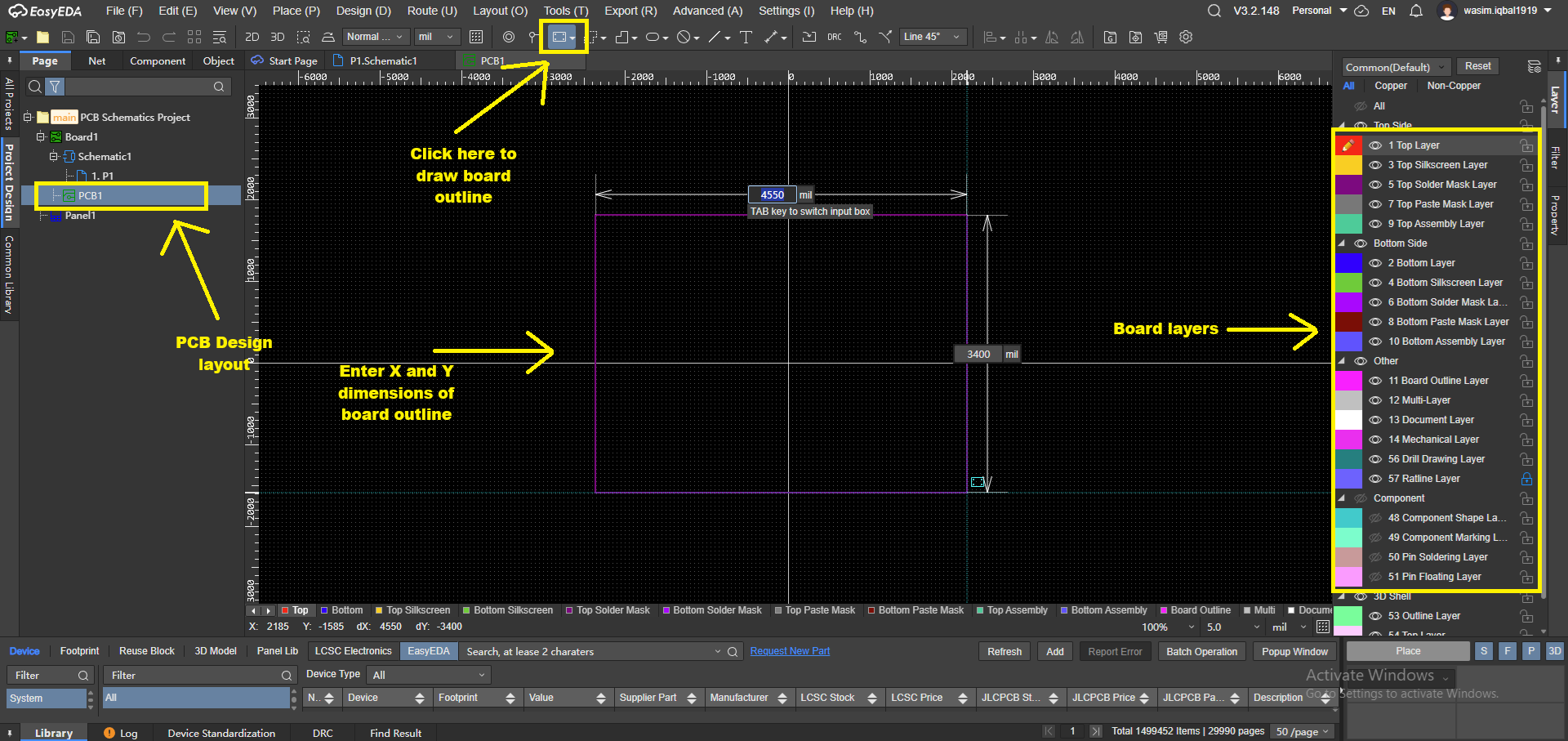
Now, place all the components required by your schematics and start interconnecting them using the wire tool. Once PCB schematics are completed, the next step is designing the board layout as shown in the figure below.
Adding Power and GND nets
Every PCB schematic requires proper power distribution. In EasyEDA, add VCC, 3V3, 5V, and GND symbols to ensure all components share the correct reference nodes. Similarly, after completing connections, properly assign reference designators to components like R1, C1, and U1, etc. Set component values and make sure all IC part numbers are correct.
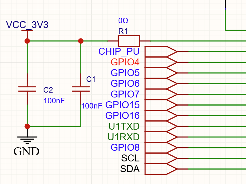
Adding Power and GND nets in PCB schematics
Assigning Net Label to Component Pins
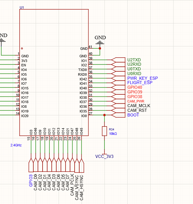
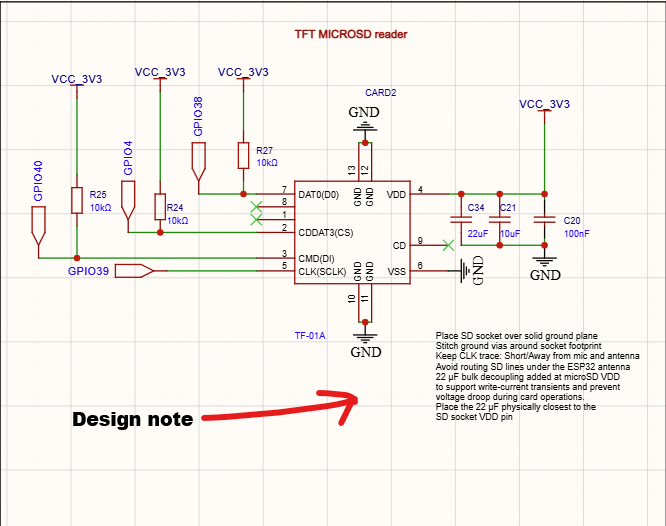
Adding comments and Design Notes
Always add the comments where appropriate in the schematics and add design notes to preserve the design intent and guide the engineers or firmware designers. A simple microSD card schematic with design notes is shown in the figure below. This will help the layout engineer in routing the board.
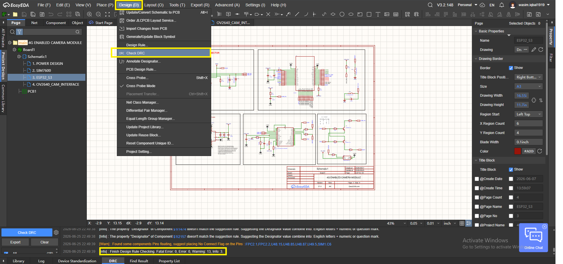
Run Electrical Rule Check (ERC)
Now, the schematics have been designed. It is time to check for any electrical errors before moving into designing the board layout. DRC will help the designer to fix missing connections or errors and resolve warnings related to floating pins or incorrect nets. Therefore, the designers must run DRC before routing the board.
If the DRC results in errors, resolve them first before moving towards the design layout of the PCB.
Converting the Schematic into PCB Layout
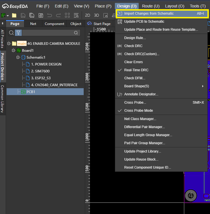
Once the schematic design has been completed and verified, the next step in the PCB design process is converting the logical circuit into a physical PCB layout. This stage transforms electrical connections, component information, and design data from the schematic into a manufacturable Printed Circuit Board (PCB).
The PCB layout stage is where components are physically placed on the board and interconnected using copper traces. While the schematic defines how the circuit should function, the PCB layout determines how that circuit will be physically implemented and manufactured.
Defining the PCB Board Outline
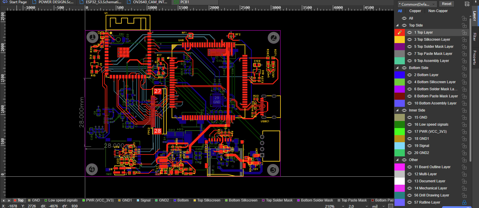
The PCB board outline defines the physical shape and dimensions of the circuit board. It serves as the boundary within which all components, traces, vias, and copper pours must fit. The board outline is typically determined by product requirements, enclosure dimensions, mounting constraints, and connector locations.
Component Placement
Component placement is one of the most critical stages of PCB design because it directly affects routing quality, signal integrity, thermal performance, and manufacturability. A good placement strategy simplifies routing and improves overall circuit performance. A sample PCB design layout is shown below with a good component placement strategy.
Routing PCB Traces
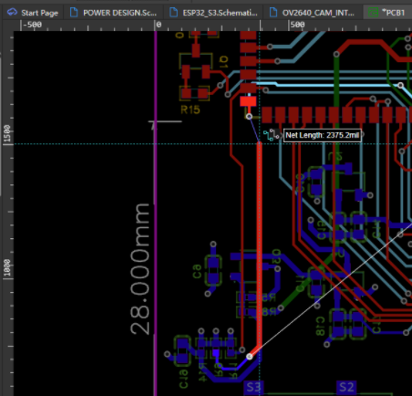
Routing is the process of creating copper connections between component pads according to the schematic netlist. Proper routing ensures reliable signal transmission and adequate current-carrying capability. For power traces carrying higher currents, wider traces should be used to reduce voltage drop and heat generation.
Creating Ground Planes and Copper Pours
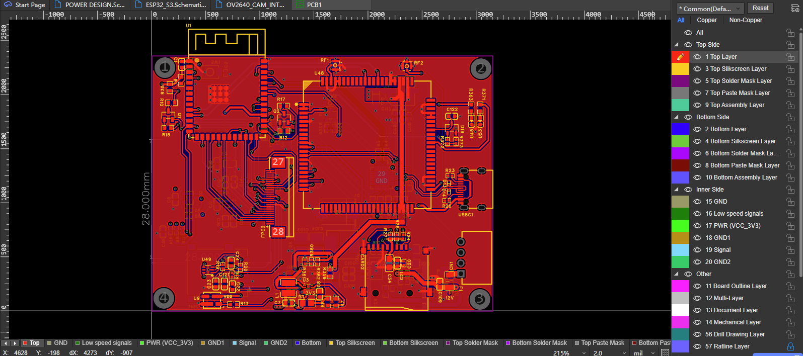
Ground planes and copper pours are large areas of copper connected to specific nets, most commonly the ground net. They play a major role in improving PCB performance and simplifying routing.
Running Design Rule Check (DRC)
After routing is complete, a Design Rule Check (DRC) should be performed to identify potential manufacturing and design issues. DRC automatically verifies that the PCB complies with predefined design constraints.
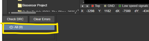
All critical DRC errors should be resolved before generating manufacturing files.
Generating Manufacturing Files
Once the PCB layout has been completed, verified, and cleared through Design Rule Check (DRC), the next step is generating the manufacturing files required for PCB fabrication and assembly. These files serve as the communication bridge between the PCB designer, PCB manufacturer, and assembly house. One of the renowned manufacturers is assembly and manufacturing is WELLER PCBs.
Gerber Files
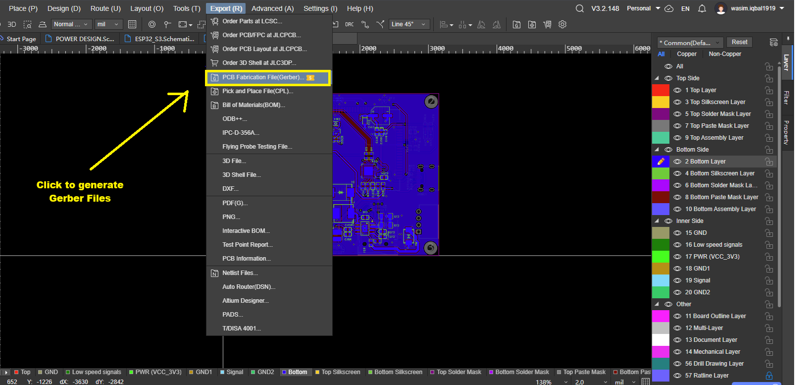
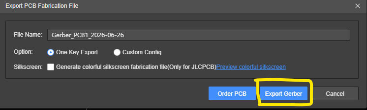
Gerber files are the industry-standard format used by PCB manufacturers to fabricate printed circuit boards. They contain graphical information that defines each PCB layer and instructs the fabrication facility how to produce the board.
| Typical Gerber Package Contents |
|---|
| Top Copper Layer |
| Top Solder Mask |
| Top Silkscreen |
| Inner Copper Layers (Multilayer PCBs) |
| Bottom Copper Layer |
| Bottom Solder Mask |
| Bottom Silkscreen |
| Board Outline Layer |
| Mechanical Layer |
These files collectively define the PCB copper layers, solder masks, silkscreen markings, board outline, and other manufacturing information required for PCB fabrication.
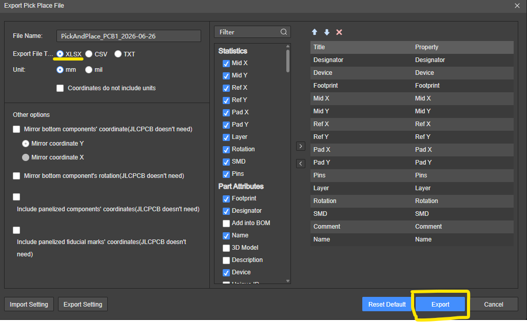
Pick and Place Files
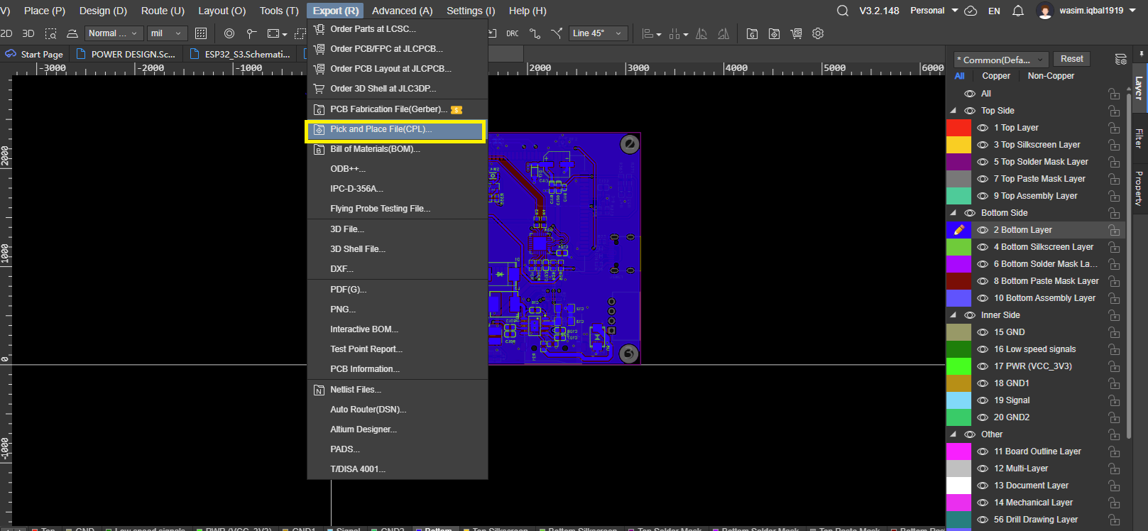
Pick-and-Place (PnP) files are used in PCB assembly to automate component placement. These files provide machine-readable information that guides automated assembly equipment when placing components on the PCB.
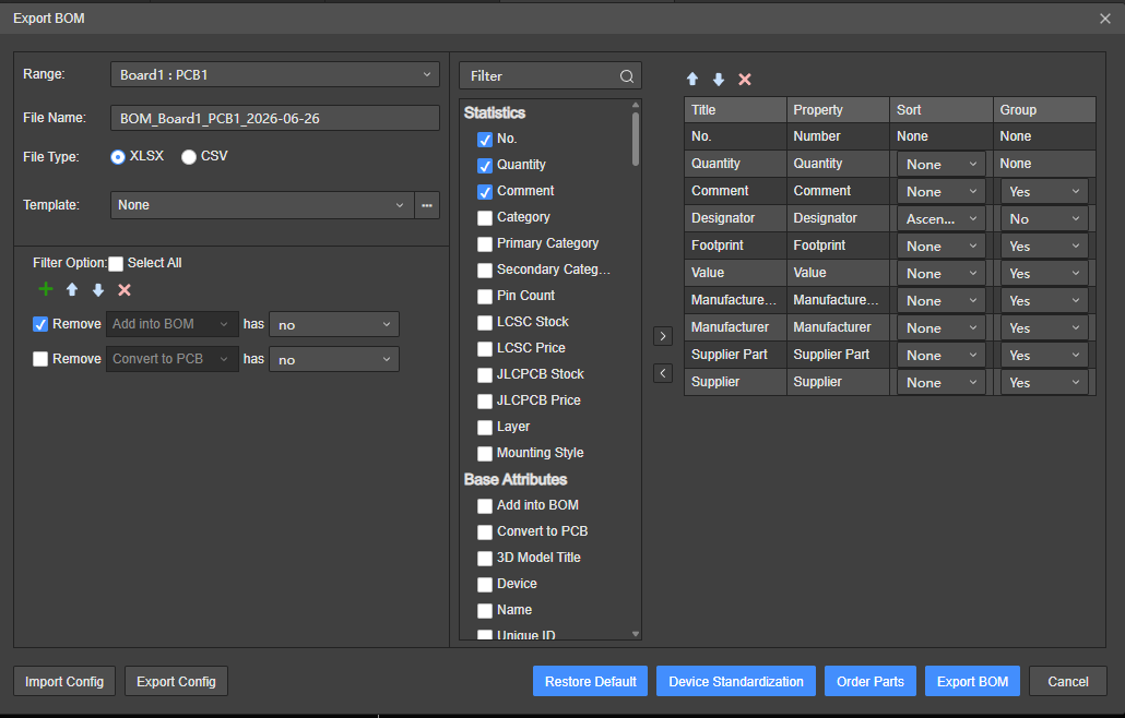
Bill of Material Files
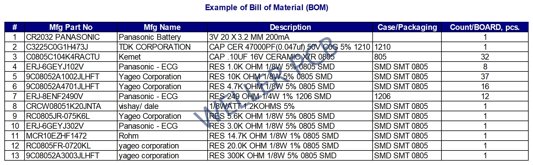
The Bill of Materials (BOM) is one of the most important manufacturing documents because it lists every component required to assemble the PCB. It serves as the primary procurement document for purchasing components and as a guide for the assembly process.
Conclusion
Designing a PCB schematic is one of the most important stages in the entire PCB development process. It forms the foundation of every electronic product by defining how components are connected and how the circuit is expected to function before moving into physical layout and manufacturing.
Throughout this guide, we explored the complete PCB design workflow, including schematic capture, component selection, library management, net connections, PCB layout conversion, and manufacturing preparation.
Frequently Asked Questions (FAQ)
A schematic shows electrical connections and circuit logic, while a PCB layout shows the physical placement of components and copper routing on the actual board.
Popular tools include Altium Designer, Cadence OrCAD, KiCad, and EasyEDA. The best choice depends on project complexity, budget, and professional requirements.
Schematic symbols represent electronic components in a circuit diagram, while libraries contain both symbols and footprints used in PCB design software.
After completing the design, engineers generate Gerber files, drill files, BOM (Bill of Materials), and pick and place files for manufacturing and assembly.
A correct schematic ensures accurate PCB layout, proper component placement, correct net connections, and ultimately error-free manufacturing and assembly.