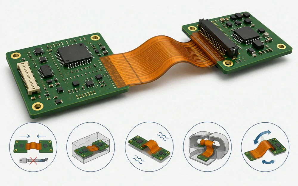
A rigid flex PCB is a packaging and reliability choice, not only a smaller way to connect two boards. Use it when cables, connectors, vibration, folding, or a tight enclosure create real design risk.
Rigid-flex can reduce connectors, save space, improve vibration resistance, and support three-dimensional layouts. It also requires early control of the stackup, bend zones, materials, assembly process, inspection plan, and installed shape.
When to Use a Rigid-Flex PCB

Rigid-flex works best when the electrical design and enclosure must operate as one system. Base the decision on product geometry, movement, reliability, assembly effort, and lifecycle cost rather than PCB price alone.
Problems Rigid-Flex Solves
A rigid-flex PCB combines rigid board areas and flexible circuit areas in one laminated structure. Rigid areas support components, connectors, shields, and dense routing. Flex areas carry signals or power through bends, corners, or stacked spaces without separate cable assemblies.
Common Applications
Typical applications include medical devices, camera modules, wearables, handheld scanners, drone gimbals, automotive sensors, aerospace electronics, RF instruments, and compact IoT equipment.
When a Rigid PCB or Cable Is Better
If one rigid PCB fits the enclosure and the connector count is low, it is usually cheaper and easier to fabricate, inspect, repair, and replace. A separate flex cable may be better when field replacement or independent module servicing is required.
Rigid PCB vs Flex PCB vs Rigid-Flex PCB
| Board Type | Best Fit | Main Advantage | Main Risk |
|---|---|---|---|
| Rigid PCB | Flat enclosures and stable mounting | Lower cost and simpler production | Split boards need cables or connectors |
| Flex PCB | Display tails and lightweight interconnects | Thin, light, and easy to route | Connectors and heavy parts need support |
| Rigid-Flex PCB | Compact products with folds or several board zones | Reduces interconnects and supports 3D packaging | Higher stackup, bending, and test risk |
Rigid Flex PCB Stackup and Materials
The stackup affects thickness, bend strain, impedance, lamination yield, and cost. Review the rigid and flexible constructions separately, then confirm which copper and dielectric layers continue through each transition.
FR-4 or high-Tg laminate is common in rigid areas, while polyimide is widely used in flex areas. Adhesiveless flex laminates can reduce thickness, but material availability and cost should be confirmed before layout release.
IPC-2223 covers flexible and rigid-flex design requirements, while IPC-6013 covers qualification and performance. State the applicable revision, performance class, installation use, material system, and acceptance criteria in the procurement documentation.
Common Stackup Options
| Total Rigid Layers | Copper Layers Through Flex | Flex Construction | Typical Application | Main DFM Risk |
|---|---|---|---|---|
| 4 | 1 | Single-sided flex | Sensors and compact controls | Limited return-path options |
| 4–6 | 2 | Double-sided flex | Medical, camera, and high-speed modules | Flex thickness and plane design |
| 8+ | 2–4 | Multilayer or HDI rigid-flex | Dense RF, imaging, and computing modules | Lamination, microvias, and yield |
This is a planning reference, not a universal construction rule. Keep only the copper layers needed in the flex section. Extra layers increase thickness and move copper farther from the neutral bend axis.
For rigid-area planning, review 4-layer PCB stackups, 6-layer options, 8-layer stackups, and HDI design limits.

RA Copper, ED Copper, and Foil Direction
Electrodeposited copper, or ED copper, can suit flex-to-install structures and limited movement. Rolled annealed copper, or RA copper, is often selected for repeated bending because it generally provides better flex endurance.
For dynamic designs, confirm the foil type, finished copper condition, plating contribution, and rolling or machine direction. Route primary conductors across the bend line and align the laminate’s preferred bending direction with the installed motion. Validate the final construction against the required cycle count.
Bend Radius and Flex Area Design Rules

Define the installed shape before component placement. Bend rules protect copper, coverlay, vias, solder joints, and rigid-to-flex transition areas from excessive strain.
Static and Dynamic Bend Conditions
A flex-to-install bend moves during assembly and then remains in position. A dynamic bend moves repeatedly during operation. Dynamic applications require a cycle target, controlled motion, fewer flex layers, suitable copper, and bend-life testing.
Static and Dynamic Bend Conditions
Dynamic bends move during use. They need a wider bend radius, thinner copper, fewer flex layers, and stronger materials.
Bend Radius Starting Points
| Flex Condition | Initial Design Reference | Required Validation |
|---|---|---|
| Flex-to-install, 1–2 copper layers | Start near 10× total flex thickness | Confirm angle, copper, coverlay, and supplier limits |
| Flex-to-install, 3+ copper layers | Start near 20× total flex thickness | Review neutral axis and layer strain |
| Dynamic bending | No universal fixed ratio | Define cycles, motion, temperature, copper, and test method |
These values are starting references, not guaranteed minimums. The approved radius depends on flex thickness, copper layers, foil type, plating, adhesive, bend angle, temperature, and service life.
Flex Area Layout Rules
- Keep components, vias, test pads, solder joints, and plated holes outside active bend areas.
- Keep copper changes, stiffener edges, and coverlay transitions away from the rigid-to-flex boundary.
- Route conductors across the bend line with curves or gentle angles.
- Avoid sudden trace-width changes inside the bend zone.
- Offset traces on adjacent flex layers instead of stacking them directly.
- Use crosshatched copper only when required and approved by the fabricator.
- Document the bend line, direction, angle, radius, installed shape, stiffeners, and coverlay openings.
For layout details, review PCB trace corner design, flex circuit stiffener design, and impedance test coupons.
Common Rigid-Flex PCB Failure Points
A board may pass bare-board electrical testing and still fail after folding, assembly, or field movement. Review mechanical risks separately from opens, shorts, and impedance.
| Failure Point | Common Cause | Risk Reduction |
|---|---|---|
| Copper cracking | Tight radius, heavy copper, or features near transitions | Increase radius and add keep-out areas |
| Short bend life | Too many flex layers or unsuitable copper | Reduce thickness and validate cycle life |
| Connector stress | Connector on unsupported flex | Move it to a rigid zone or add a stiffener |
| Delamination or blistering | Moisture or excessive thermal exposure | Control storage, drying, and soldering |
| Wrong installed shape | Missing or unclear bend drawing | Provide a drawing and STEP model |
Rigid Flex PCB DFM Checklist
| DFM Item | What to Confirm | Why It Matters |
|---|---|---|
| Bend definition | Line, direction, angle, radius, cycles, and installed shape | Prevents uncontrolled movement |
| Stackup | Rigid layers, flex layers, copper, dielectric, adhesive, and coverlay | Controls thickness, impedance, and bend life |
| Transition zones | Clearance from vias, pads, copper changes, and stiffeners | Reduces stress concentration |
| Coverlay | Openings, registration tolerance, and exposed pads | Prevents insulation and soldering problems |
| Stiffeners | Material, thickness, outline, adhesive, and edge position | Supports connectors without adding stress |
| Controlled impedance | Geometry, reference layer, tolerance, coupon, and test method | Controls high-speed and RF links |
Manufacturing, Assembly, and Testing

Rigid-flex production includes drilling, plating, lamination, coverlay, solder mask, routing, electrical testing, and inspection. Assembly also needs controlled support because flex areas can move during printing, placement, reflow, and handling.
Moisture Control Before Assembly
Polyimide absorbs moisture from normal air exposure. During soldering, trapped moisture can contribute to blistering, delamination, tearing, or interface damage. Storage and drying must therefore be part of the assembly plan.
Keep boards in controlled packaging and minimize the time between drying and soldering. Do not use one universal bake profile. Qualify the process for the laminate system, copper distribution, board thickness, packaging history, storage time, drying equipment, and planned soldering cycles.
Match Each Test to a Specific Risk
| Method | What It Verifies | What It Does Not Fully Verify |
|---|---|---|
| AOI | Patterns, coverlay registration, and visible defects | Internal lamination or bend life |
| Electrical test | Opens, shorts, continuity, and isolation | Mechanical life after bending |
| Microsection | Plating, vias, dielectric, and lamination quality | Full-board installed motion |
| Bend-cycle test | Durability at a defined radius and cycle count | Production-wide electrical conformity |
| TDR coupon | Controlled impedance against the approved stackup | Mechanical stress in the enclosure |
| Functional test | Assembly operation under defined coverage | Long-term field life unless designed for it |
Use the test combination that matches the actual risks. For visible process control, review how AOI supports PCB yield and inspection.
Cost Drivers and Quote File Requirements
Cost depends on flex layers, materials, copper type, impedance control, stiffeners, testing, and manufacturing yield.
| Cost Driver | Why Cost Increases | Lower-Risk Reduction |
|---|---|---|
| More flex layers | More thickness, lamination, and bend risk | Keep only required signals in flex |
| HDI and microvias | More drilling, plating, and yield sensitivity | Use HDI only where density requires it |
| Controlled impedance | Tighter stackup, coupons, and testing | Control only specified signals |
| Dynamic flexing | Special materials and bend-life validation | Separate dynamic and static zones |
Files Needed for a Rigid Flex PCB Quote
- Gerber or ODB++ data, drill files, netlist, outline, and stackup drawing.
- Bend line, direction, angle, radius, cycle target, and installed-shape drawing.
- Material, copper type and thickness, finish, coverlay, solder mask, and stiffener notes.
- Impedance table, tolerance, reference layers, and coupon requirements.
- BOM, pick-and-place data, assembly drawings, and STEP files.
- Performance class, installation use, inspection, electrical test, and bend-test requirements.
How to Finalize a Reliable Rigid-Flex PCB Design
Rigid-flex is appropriate when it removes risky connectors, fits a constrained enclosure, withstands vibration, or supports a controlled three-dimensional assembly. It is not automatically better when a rigid PCB or replaceable cable can meet the same requirements with less manufacturing and service risk.
Before prototype release, finalize the layer definitions, copper type, bend radius, transition keep-outs, installed shape, moisture-control plan, fixtures, and test coverage. Ask the fabricator to review the stackup, bend zones, coverlay, stiffeners, impedance structures, and drawing notes before production data is frozen.
For dynamic motion, high-speed signals, HDI, BGAs, or tight packaging, send the complete fabrication and mechanical files for early DFM review. Request a rigid-flex PCB review and quote when the design package is ready.

FAQ
What is the difference between a rigid flex PCB and a flex PCB?
A flex PCB is bendable. A rigid-flex PCB combines flexible interconnect areas with rigid areas that support components, connectors, mounting holes, and dense routing.
When should you use rigid-flex instead of connectors?
Use it when connectors add unacceptable space, weight, assembly steps, vibration risk, or signal discontinuity. Use a cable when replacement and module servicing are more important.
Can components be placed on a flex area?
Components should normally remain on rigid areas. When flex-area placement is unavoidable, review the stiffener, solder joints, strain relief, and installed movement.
What is the minimum bend radius for a rigid-flex PCB?
There is no universal minimum. It depends on flex thickness, copper layers, foil type, plating, bend angle, temperature, motion, and required cycle life.
How much does a rigid flex PCB cost?
Cost depends on the board size, layer count, materials, copper type, stiffeners, testing, and special features such as HDI or impedance control.
What causes most rigid flex prototype delays?
Most delays happen when important details are missing. These may include the bend drawing, stackup, STEP file, impedance needs, or fixture plan.
Post Views: 49