The role of AOI in PCB design extends far beyond the factory floor. By integrating Automated Optical Inspection (AOI) considerations early in the design phase, engineers can significantly improve PCB manufacturing and assembly yield and prevent costly defects. This article explores how AOI influences PCB layout, component placement, and overall product reliability.
The Role of Automated Optical Inspection (AOI) Technology in PCB Design
Printed circuit boards have become increasingly compact, complex, and performance-critical, making defect prevention a major priority in modern electronics development. As component densities rise and tolerances shrink, traditional manual inspection methods struggle to keep pace. This is where Automated Optical Inspection (AOI) has become indispensable.
AOI is often associated with manufacturing and assembly, but its role extends much deeper into PCB design itself. It influences how boards are designed, how defects are prevented, how manufacturability is improved, and ultimately how product reliability is achieved. Rather than serving only as a post-production checkpoint, AOI has evolved into an essential contributor to quality-driven PCB design.

What Is the **Role of AOI in PCB Design** and Manufacturing?
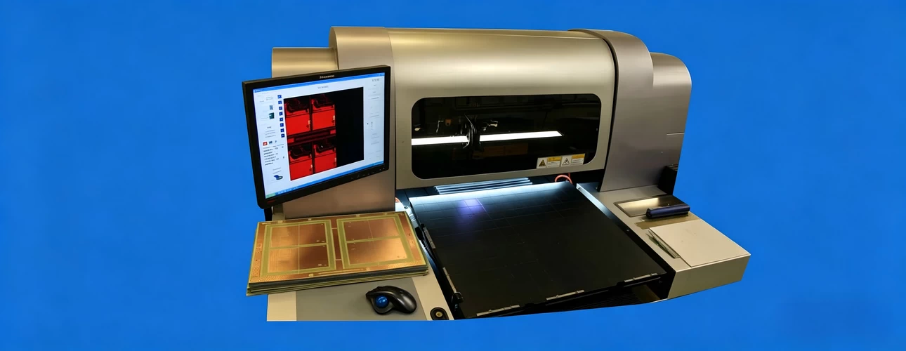
Automated Optical Inspection is a visual inspection technology that uses cameras, lighting systems, and image processing software to detect defects on bare PCBs and assembled boards.
AOI systems are non-contact systems that compare inspected boards against a “golden board,” design database, or programmed rules to identify deviations.
These systems can detect defects such as:
- Missing or misplaced components (assembled PCB)
- Solder bridges (assembled PCB)
- Insufficient or excess (assembled PCB)
- solder (assembled PCB)
- Polarity errors (assembled PCB)
- Open circuits and shorts (bare PCB)
- Trace width or spacing defects (bare PCB)
- Surface scratches and etching issues (bare PCB)

Modern AOI systems may use 2D or 3D imaging, with 3D AOI particularly valuable for solder volume measurement and height analysis. AOI improves consistency by automating inspections that would otherwise depend on human judgment, speed, and attention.
Suggested Reading: Top 10 DFM Issues that Affecting PCB Manufacturing
How **AOI in PCB Design** Prevents Defects Early
Although often implemented during manufacturing, AOI begins influencing product quality during the design stage.
Design for Inspection
A well-designed PCB is easier to inspect. Designers often consider AOI compatibility when placing components, defining pad geometries, selecting spacing, and arranging testable layouts.
For example, components placed too close together may increase false calls or make optical inspection more difficult. Similarly, poor silkscreen placement or unclear markings can hinder defect detection.

This is where AOI supports Design for Manufacturability (DFM) and Design for Testability (DFT) principles. By designing with inspection in mind, engineers reduce both manufacturing risk and downstream defect escapes.

Catching Design-Related Issues Early
AOI can also help expose defects rooted in design rather than assembly.
Examples include:
- Inadequate pad designs causing soldering problems
- Trace spacing issues that increase short risk
- Incorrect footprints
- Polarity marking errors
- Component orientation problems
When these issues are detected through prototype or early production AOI feedback, designs can be improved before scaling to volume manufacturing.
In this way, AOI contributes not just to defect detection, but to design optimization.
Suggested Reading: Avoid PCB Fab Errors: Why Your Fabrication Drawing is Critical
How AOI Works in PCB manufacturing
AOI systems generally rely on three key elements:
1. High-Resolution Imaging
High-resolution cameras capture detailed images of the PCB surface. Multiple viewing angles and specialized lighting help reveal defects that may be hard to detect manually.
2. Image Comparison and Analysis
Software compares captured images against design references or known-good samples. Common inspection approaches include:
- Rule-based inspection
- Golden board comparison
- Pattern matching
- Statistical image analysis
3. Defect Classification
Potential defects are flagged for review, allowing operators to confirm and correct issues. It saves time as most issues are dealt with on the assembly line, evading costly rework and repairs.
Many systems now include machine learning algorithms that reduce false positives and improve detection performance. The speed and repeatability of this process make AOI especially valuable for high-density and high-volume electronics production.
Which Defects Can AOI Prevent?
One of AOI’s biggest contributions to PCB reliability is early defect detection.
Soldering Defects
Solder-related issues are one of the most common causes of assembly defects. Thanks to AOI, these issues can be automatically identified at the assembly stage. Typical solder issues caught in AOI inspection include:
- Cold joints
- Bridging
- Tombstoning
- Insufficient solder
- Lifted leads
Finding these defects early prevents expensive downstream failures.
Component Placement Errors
Incorrectly placed components can cause functional failures even when soldering appears acceptable.
AOI checks assembled boards while focusing on:
- Presence or absence
- Rotation errors
- Misalignment
- Wrong component
- placement
For modern surface mount assemblies, these checks are critical.
Bare Board Defects
AOI is also used before assembly to detect fabrication defects such as:
- Opens and shorts
- Trace defects
- Etching errors
- Registration problems

Catching these issues before assembly saves significant cost.
Quality Control with AOI
AOI is often considered one of the strongest quality control tools in PCB production because it supports both defect detection and process improvement. The following table summarize how AOI helps quality control in PCB inspection.
AOI Benefit
Description
Example / Impact
Process Feedback
AOI does more than identify defective boards; it generates inspection data that helps uncover recurring process issues and supports continuous improvement.
Defect trends may reveal pick-and-place calibration errors, solder paste printing issues, reflow profile problems, or even design weaknesses. For example, repeated solder bridging on a specific footprint may indicate a pad design issue rather than an assembly problem.
Reduced Human Error
AOI improves inspection consistency by applying the same criteria to every board, unlike manual inspection which may vary between operators.
Particularly valuable for miniaturized components and complex PCB assemblies where manual inspection can miss subtle defects.
Higher Production Yield
Early defect detection reduces scrap, rework, and defective boards moving to later stages of production.
Improved process control leads to higher manufacturing yield and lower production costs.
AOI and Reliability in High-Reliability Electronics
AOI plays a particularly important role in industries where failures have serious consequences.
Automotive Electronics
Advanced driver assistance systems, battery management boards, and control modules demand extremely high assembly quality. AOI helps support zero-defect goals in these applications.
Medical Devices
Reliability is critical in diagnostic and patient-support electronics, making rigorous inspection essential.
Aerospace and Defense
High-density, mission-critical electronics often combine AOI with additional methods such as X-ray and functional testing for layered quality assurance.
In these sectors, AOI supports broader reliability strategies rather than acting as a standalone tool.
Limitations of AOI
AOI plays a particularly important role in industries where failures have serious consequences.
It has limitations.
Hidden Defects
AOI relies on line-of-sight inspection
It may struggle with:
- Hidden solder joints (such as BGAs)
- Internal layer defects
- Via integrity issues
- Subsurface failures
These often require complementary techniques such as X-ray inspection or electrical testing.
Functional Performance
AOI verifies appearance and many physical defects, but it does not prove electrical functionality. A visually correct board can still fail functionally. This is why AOI is typically used alongside in-circuit testing (ICT) and functional testing.
False Calls
AOI systems can sometimes flag acceptable conditions as defects.
While modern algorithms reduce false positives, programming and optimization remain important.
Understanding these limitations is essential to using AOI effectively.
AOI and Advanced PCB Manufacturing Technologies
As PCB technologies advance, AOI has become even more important.
High-Density Interconnect (HDI) Boards
As PCBs shrink in size, the component placement becomes denser with time. It therefore requires fine-pitch components and tighter spacing in PCBs. Consequently, it increases defect risks while making manual inspection less practical. AOI provides the precision needed for these assemblies as it’s a non-contact form of inspection method.

Flex and Rigid-Flex PCBs
Rigid flex PCBs are becoming a norm thanks to wearable devices and lightweight electronic equipment. These introduce additional inspection challenges related to material movement and geometry. AOI helps improve consistency in these specialized designs.

Further Reading: What Is a Rigid-Flex PCB? Benefits, Design Tips, and Applications
3D AOI
Traditional 2D systems focus largely on appearance.
3D AOI adds measurement capabilities for:
- Solder volume
- Coplanarity
- Component height
- Lead lift detection
This expands defect coverage significantly.
Emerging Trends in AOI
AOI continues evolving alongside smart manufacturing.
AI-Driven Inspection
Artificial intelligence is improving defect recognition while reducing false calls.Likewise, Deep learning approaches are increasingly used for complex defect classification.
Data-Driven Quality Analytics
AOI is becoming part of broader manufacturing analytics systems where inspection data supports predictive quality control.
Industry 4.0 Integration
Connected factories increasingly link AOI systems with process monitoring and automated feedback loops.
Rather than simply detecting defects, AOI is becoming part of intelligent manufacturing ecosystems.
Conclusion
As electronic products continue becoming smaller, faster, and more complex, maintaining quality requires more than traditional inspection methods. Automated Optical Inspection has become a foundational technology in modern PCB design and manufacturing. It helps detect defects early, improve process control, support reliability, and reinforce design quality from prototype through production.
While AOI is not a replacement for electrical testing or reliability validation, it is a critical layer in a comprehensive quality strategy. For today’s advanced electronics, AOI is not simply an inspection tool—it is an enabler of better PCB design.
Frequently Asked Questions
1. What is AOI in PCB design?
AOI, or Automated Optical Inspection, is a machine vision-based inspection method used to detect visual defects on bare and assembled PCBs. It helps improve quality, manufacturability, and reliability.
2. What defects can AOI detect?
AOI can detect missing components, polarity errors, solder bridges, insufficient solder, open circuits, shorts, trace defects, and component placement problems.
3. Is AOI used only after PCB assembly?
No. AOI can be used during bare board fabrication, solder paste inspection, component placement verification, and post-reflow inspection.
4. Can AOI replace electrical testing?
No. AOI identifies visual and physical defects but does not verify electrical functionality, so it is usually used alongside ICT or functional testing.
5. Why is AOI important for high-density PCB designs?
High-density designs use smaller components and tighter tolerances, making manual inspection difficult. AOI provides the precision and consistency needed to inspect these complex boards effectively.
References
- “Automated Optical Inspection (AOI),” PCBWay, [Online]. Available: https://www.protoexpress.com/kb/automated-optical-inspection/
- “Leading PCB AOI machine manfacturing,” Orbotech Ltd , [Online]. Available: https://www.kla.com/media-room/channels/innovation/orbotech-innovation
- “Automated Optical Inspection,” MCLPCB, [Online]. Available: https://www.mclpcb.com/blog/automated-optical-inspection/
- “Why AOI and Quality Control Matter in PCB and Flex PCB,” PICA Manufacturing, [Online]. Available: https://picamfg.com/why-aoi-and-quality-control-matter-in-pcb-and-flex-pcb/
- “Automated Optical Inspection,” Wevolver, [Online]. Available: https://www.wevolver.com/article/automated-optical-inspection


