
Modern electronic systems are increasingly required to handle high voltages —from renewable energy converters and electric vehicles to medical imaging systems and industrial automation. Designing printed circuit boards (PCBs) that safely and reliably operate at high voltage levels demands more than standard design rules.
A high-voltage PCB (HV-PCB) must prevent arc discharge, dielectric breakdown, and long-term insulation degradation while maintaining electrical performance and manufacturability. Understanding clearance, creepage, insulation coordination, and the correct use of slots or barriers is fundamental to achieving robust designs.
This article explores the technical and practical principles of high-voltage PCB design, covering physical spacing rules, material properties, design optimization techniques, and relevant international standards.
What are Electrical Stresses in High-Voltage PCBs
High voltage creates intense electric fields between conductive features. If the electric field strength exceeds the breakdown voltage of the insulating medium, an electrical discharge or insulation failure can occur.
There are two primary failure modes:
- Air Breakdown (Arcing): A flashover through air due to insufficient clearance between conductors.
- Surface Tracking: Conductive paths forming along the PCB surface under voltage stress, often worsened by contaminants or humidity.
To prevent these failures, designers must properly define clearance (through-air distance) and creepage (along-surface distance), supplemented by proper insulation materials and geometric techniques such as slots and barriers.

Clearance and Creepage
Clearance and Creepage
Clearance is the shortest distance through air between two conductive parts. It ensures that air insulation is never overstressed. The required clearance depends mainly on:
- Working voltage and surge voltage
- Pollution degree (environmental contamination)
- Altitude (lower air pressure reduces dielectric strength)
- Overvoltage category (based on IEC 60664)
Breakdown of air typically occurs at around 3 kV/mm at sea level, but design allowances reduce this value significantly for safety and manufacturing tolerances.
Suggested Reading: PCB Trace Width VS Current Value Calculator
Creepage
Creepage distance is the shortest path along the surface of insulating material between conductors. Contaminants, moisture, and surface imperfections can lower surface insulation strength, making creepage crucial for long-term reliability.
A useful indicator is the Comparative Tracking Index (CTI) of the material
- CTI > 600: Excellent (e.g., ceramic, PTFE)
- CTI 400–600: Good (high-grade FR-4, polyimide)
- CTI < 175: Poor insulation performance
The higher the CTI, the smaller the required creepage for a given voltage level.
Recommended Reading: What Is CTI in PCB Base Materials? Meaning and Importance Explained
How Clearance and Creepage are Related
Clearance controls flashover through air. On the other hand, creepage controls tracking along surfaces. Both must be considered independently.
In most standards, creepage is usually greater than clearance unless the design uses conformal coatings or potting materials that improve surface insulation.
International Standards Governing Spacing
Designers rely on international standards to determine safe spacing values. The most important standards include:
| Standard | Scope | Application |
|---|---|---|
| IPC-2221B | General PCB design standard | Defines base spacing guidelines |
| IEC 60664-1 | Insulation coordination | Defines creepage and clearance for equipment below 1000 V AC or 1500 V DC |
| UL 60950-1 / IEC 60950-1 | IT equipment safety | Establishes spacing and insulation rules |
| IEC 61010-1 | Measurement & laboratory equipment | High-voltage equipment |
| UL 840 | Insulation systems | Defines pollution degree, CTI classes, and insulation materials |
For quick reference, IPC-2221B spacing guidelines (material group III, pollution degree 2) are summarized below:
| Working Voltage (VRMS/DC) | Minimum Clearance (mm) | Minimum Creepage (mm |
|---|---|---|
| 0–30V | 0.1 | 0.1 |
| 31–150 V | 0.6 | 1.0 |
| 151–300V | 1.2 | 1.6 |
| 301–600V | 2.4 | 3.2 |
| 601–1000V | 4.8 | 6.4 |
Suggested Reading: The Difference between IPC-6012, IPC-A-600, and IPC-A-610
Material Considerations for High-Voltage PCBs
Substrate Materials
The dielectric properties of the substrate dictate the insulation capability. The dielectric breakdown strength and loss tangent are critical metrics.
| Material | Typical Breakdown Strength (kV/mm) | CTI | Notes |
|---|---|---|---|
| FR-4 | 20–40 | 175–300 | Low cost, limited for >1.5 kV |
| Polyimide | 100+ | >400 | Excellent for aerospac |
| PTFE (Teflon) | 60–100 | >600 | Excellent dielectric, low loss |
| Ceramic-filled IMS | 40–60 | >600 | Excellent heat and voltage tolerance |
In high-frequency, high-voltage systems like RF power modules or solid-state transformers, PTFE or ceramic-filled substrates are preferred.
Recommended Reading: Meeting the Demands of 5G: A Guide to High-Frequency PCB Materials and Design
Copper Thickness & Surface Finish
Thicker copper (e.g., 2–4 oz/ft²) increases current-carrying capacity. At the same time, it reduces spacing flexibility.
Likewise, smooth finishes such as ENIG reduce field concentration compared to rougher surfaces. Moreover, rounded trace corners are also crucial to minimize electric field enhancement points.
Design Implementation Techniques
Here are some useful techniques to employ during the design phase:
Design Implementation Techniques
When laying out high-voltage circuitry:
- Keep high-voltage nets isolated from low-voltage control sections.
- Use guard rings or grounded copper shields to confine electric fields.
- Define no-routing zones near HV components to maintain clearance.
Design tools such as Cadence Allegro and Altium Designer allow voltage-based clearance rules for automated checking and spacing enforcement.
Use of Slots and Barriers
Slots are cutouts through the PCB dielectric. They effectively increase surface path length (creepage) without adding board size.
They are particularly beneficial between:
- Primary and secondary sides in SMPS transformers.
- High-voltage connectors and low-voltage sensor inputs.
For optimal slot implementation, here are some useful design guidelines: - Slot width should be at least 1 mm for manufacturing reliability.
- Keep slot edges smooth to prevent localized field intensification.
- Consider plated vs. non-plated options; non-plated slots are preferred for isolation paths.
Generally, slots are applied in isolation barriers, which improves compliance with reinforced insulation requirements under IEC/UL standards.
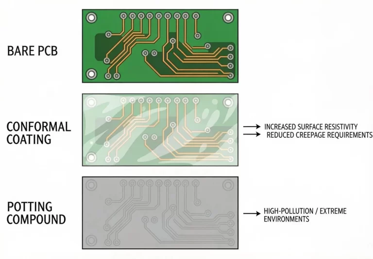
Conformal Coating & Potting
A conformal coating (e.g., silicone, acrylic) increases surface resistivity and prevents contamination. It can reduce required creepage by 25–50%, depending on the certification.
Potting compounds, used in extreme environments, create complete encapsulation and are often required for Pollution Degree 3 or 4 conditions.
Multilayer and Internal Layer Spacing
Internal PCB layers are inherently insulated by dielectric material, so their required spacing is based on dielectric thickness, not IPC clearance distances. However, ensure high-voltage nets on buried layers are separated by adequate laminate thickness—e.g., ≥0.4 mm for 600 V.
Suggested Reading: 8-Layer PCB Stackup Design Guidelines: Best Practices & Reference
Thermal and Mechanical Design
High-voltage components often dissipate significant heat. Using ceramic-filled IMS or DBC (Direct Bonded Copper) substrates combines insulation strength with high thermal conductivity (1–24 W/m·K).
It’s also best to avoid overreliance on FR-4 when both thermal and dielectric demands are high.
Recommended Reading: PCB Thermal Dissipation Solutions: A Guide to Managing High Power Designs
Insulation Systems
Insulation systems in PCB design ensure electrical isolation between conductive elements to prevent short circuits and arcing. They play a crucial role in maintaining safety, reliability, and performance under varying voltage and environmental conditions.
Insulation Systems
According to IEC 60664 and UL 840, the following insulation measures must be taken for high-voltage PCB designs.
- Functional insulation: Required for operation but not for safety
- Basic insulation: A single layer preventing electric shock.
- Supplementary insulation: Independent backup for basic.
- Double insulation: Basic + supplementary combined.
- Reinforced insulation: Equivalent to double insulation by one system.
In high-voltage PCBs, reinforced insulation is mandatory between primary (HV) and secondary (LV) circuits — for example, in isolated DC/DC converters or chargers.
Breakdown Scenarios to Watch
- Corona Discharge: Occurs at high fields (>3 kV/mm) around sharp copper edges.
- Partial Discharge: Localized discharges under coatings that degrade insulation.
- Thermal Runaway: When heat buildup weakens dielectric properties.
- To mitigate these issues, the following measures are highly effective:
- Manage a radius of at least 0.25 mm
- Maintain dry surfaces
- Ensure uniform coating thickness.
Suggested Reading: How Temperature and Humidity Can Damage Your PCB
Conclusion
Designing high-voltage PCBs demands a holistic approach combining electrical, mechanical, and materials engineering principles. Clearance and creepage define the physical limits preventing breakdown, while slots, coatings, and reinforced insulation ensure longevity under real-world conditions.
Industry adherence to IPC, IEC, and UL standards ensures both compliance and reliability. For students, a solid understanding of these concepts lays the groundwork for designing power electronics that balance safety, performance, and manufacturability.
With the growing trend towards electrification and compact high-power systems, mastering high-voltage PCB design is not just beneficial—it’s essential.
Frequently Asked Questions
1. What is the difference between clearance and creepage in PCBs?
Clearance is the shortest path through air between conductive parts, while creepage is the shortest path along an insulating surface. Clearance prevents arcing; creepage prevents surface tracking.
2. How does conformal coating affect spacing requirements?
A properly applied coating can reduce required creepage distances by 25–50%, as it limits surface contamination and moisture absorption.
3. What role do slots play in high-voltage PCB design?
Slots extend the creepage path without increasing board size, enhancing insulation between high-voltage and low-voltage sections.
4. Can FR-4 be used for high-voltage designs over 5 kV?
Generally no. FR-4’s breakdown strength (~20–40 kV/mm) and low CTI make it unsuitable for reliable operation above 2–3 kV unless reinforced or coated. Specialized materials like polyimide or PTFE are preferred.
5. What tests ensure PCB insulation reliability?
Key tests include HiPot (dielectric strength), partial discharge detection, insulation resistance measurement, and long-term thermal cycling.
References
- PICA Manufacturing, High‑Voltage PCB Design Guidelines: Key Layout and Material Considerations, 2025. Available: https://www.picamfg.com/designing-high-voltage-pcbs/
- VSE Electronics, Creepage and Clearance Standards for High‑Voltage PCBs, 2025. Available: https://www.vse.com/blog/creepage-and-clearance-rules-for-high-voltage-boards/
- NCAB, “How to optimize EMC performance in PCB design & manufacturing,” https://www.ncabgroup.com/blog/optimize-emc-performance-in-pcb-design/
- Texas Instruments, “Demystifying clearance and creepage distance for high‑voltage PCB design,” Texas Instruments Application Report SLUP419, 2023. [Online]. Available: https://www.ti.com/lit/ml/slup419/slup419.pdf
- Altium, “Using an IPC‑2221 calculator for high‑voltage design,” Altium Resources, 2020. [Online]. Available: https://resources.altium.com/p/using-an-ipc-2221-calculator-for-high-voltage-design


