
Introduction: The Invisible Threats to PCB Reliability
Printed Circuit Boards (PCBs) are the backbone of modern electronics, but their reliability faces constant challenges from two pervasive environmental factors: temperature and humidity. These invisible threats operate silently during manufacturing, storage, and throughout a product’s lifecycle, potentially causing catastrophic failures in seemingly robust electronic assemblies.
Understanding how these factors damage PCBs isn’t just theoretical knowledge—it’s essential for preventing field failures, reducing warranty costs, and ensuring your products meet their expected lifespan. This guide examines the specific damage mechanisms, provides real-world examples, and offers practical prevention strategies from both manufacturing and design perspectives.
Section 1: Thermal Damage Mechanisms in PCBs
Thermal Cycling and Fatigue Failure
Solder Joint Cracking:
The most common failure occurs where component leads meet solder joints. Repeated thermal cycling causes work hardening and eventual fracture, particularly in lead-free solder alloys that are inherently less ductile.
Copper Trace Damage:
Dissimilar expansion between copper traces and the FR-4 substrate can cause traces to delaminate or crack, especially at sharp corners or vias.
Plated Through-Hole (PTH) Barrel Cracking:
The difference in CTE between the copper barrel and the surrounding laminate creates hoop stresses that can rupture the connection.
Extreme Temperature Exposure
Beyond cycling, sustained exposure to high or low temperatures presents distinct challenges:
High-Temperature Degradation:
Prolonged exposure above a PCB's Glass Transition Temperature (Tg)—the point at which the substrate changes from rigid to rubbery—causes permanent deformation, loss of mechanical strength, and chemical breakdown of the resin system.
Low-Temperature Embrittlement:
At extremely low temperatures, materials become brittle. Solder joints lose their ability to absorb stress through plastic deformation, making them susceptible to shock-induced fracture.
Section 2: Humidity and Moisture-Related Failures
The Process of Moisture Absorption
PCB substrates, particularly FR-4, are hygroscopic. They absorb moisture from the atmosphere during storage and assembly. This absorbed water becomes problematic during the high-temperature reflow soldering process in SMT assembly.
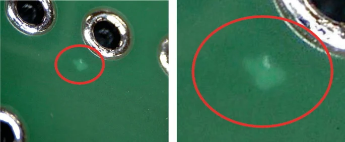
Popcorning" and Delamination
When trapped moisture rapidly vaporizes during reflow (typically at temperatures above 220°C), it creates internal pressure. This can cause:
Internal Delamination:
Separation of the copper layers from the substrate or separation within the laminate layers themselves.
"Popcorning" of Components:
Moisture absorbed by plastic-encapsulated IC packages (like BGAs and QFNs) vaporizes, cracking the package and destroying the chip. This is a major concern in SMT assembly.
"Popcorning" of Components:
Moisture absorbed by plastic-encapsulated IC packages (like BGAs and QFNs) vaporizes, cracking the package and destroying the chip. This is a major concern in SMT assembly.
Conductive Anodic Filament (CAF) Formatio
A related, sub-surface failure occurs along the glass fiber/epoxy resin interface inside the PCB. In the presence of humidity, voltage, and ionic contamination, copper can migrate along these paths, creating hidden shorts between adjacent vias or traces that are impossible to detect visually.

Section 3: The Combined Attack – Temperature Humidity Bias (THB) Testing
Industry standards like IPC-TM-650 simulate the worst-case scenario with Temperature Humidity Bias (THB) Testing. Boards are subjected to high temperature (e.g., 85°C), high humidity (e.g., 85% RH), and continuous electrical bias. This accelerated test reveals weaknesses in material selection, laminate quality, and cleanliness that would otherwise take years to manifest in the field.
Section 4: Prevention Strategies for Manufacturing and Design
Manufacturing & Storage Controls
Moisture-Sensitive Device (MSD) Handling:
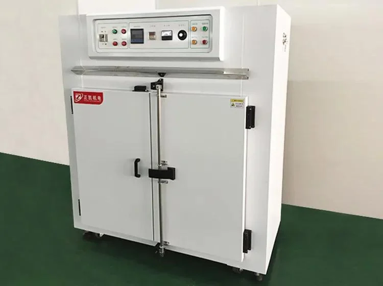
Strict adherence to IPC/JEDEC J-STD-033. This includes proper dry packaging, tracking exposure time (floor life), and mandatory baking before reflow for components removed from their dry bags.
Environmental Controls:
Maintain storage and assembly areas at stable, low-humidity conditions (ideally below 40% RH) with controlled temperature.
Process Cleanliness:
Implement effective post-solder cleaning to remove ionic flux residues that facilitate electrochemical migration. Use low-residue or no-clean fluxes appropriately.
Proper Curing and Baking:
Ensure laminates and conformal coatings are fully cured, and bake PCBs prior to assembly if moisture absorption is suspected.
Design for Reliability (DFR)
Material Selection:
Choose substrates with higher Tg and lower moisture absorption rates for harsh environments. Consider polyimide or specialized low-loss laminates for high-reliability applications.
Conformal Coating:
Apply acrylic, silicone, urethane, or parylene coatings to create a physical barrier against moisture and contaminants.
Increased Spacing:
In high-humidity applications, increase conductor spacing (creepage and clearance) to mitigate risks of electrochemical migration and CAF.
Robust Layout:
Avoid sharp corners in traces that concentrate stress. Use tear-drop pads at vias to improve mechanical strength.
Conclusion: An Ounce of Prevention
Temperature and humidity are not merely environmental conditions; they are active agents of PCB degradation. The damage they cause—from cracked solder joints and popped components to dendritic growth and hidden shorts—is predictable and, therefore, preventable.
Successful prevention requires a holistic approach, integrating vigilant manufacturing process controls, intelligent material selection, and foresighted design practices. By understanding these failure mechanisms and implementing the strategies outlined above, manufacturers and designers can significantly enhance PCB reliability, reduce costly field failures, and build electronics that endure.
Investing in this understanding is ultimately an investment in your product’s reputation and your bottom line.


