
The PCB manufacturing and design market is booming and expected to become a $100 billion industry by 2030. This growth comes from highly in-demand areas like IoT gadgets, electric cars, and 5G networks. Understandably, PCBs are the key backbone in these systems, connecting sensors, chips, and power parts into small, powerful boards that make modern electronics work.
Modern PCB design tools like Altium 365, KiCad, and Autodesk Eagle are changing everything for industries looking to outsource PCB services. By using smart AI tools, they cut 50 to 70% design time. So, weeks of hands-on work can now be completed in hours using simple automation techniques.
Thanks to this automation, you can:
- Build tricky multi-layer boards packed with components
- Handle fast signals
- Check heat issues
Most importantly, you can achieve all of it while complying the standards like IPC-2221 for high-power setups.
So, if you’re an industry pro needing quick, reliable boards from service providers, this article shows how these tools speed up projects, save money, and improve quality. Find out the insights about auto-checks, 3D previews, team sharing online, and tips to pick the best design services for your next build.

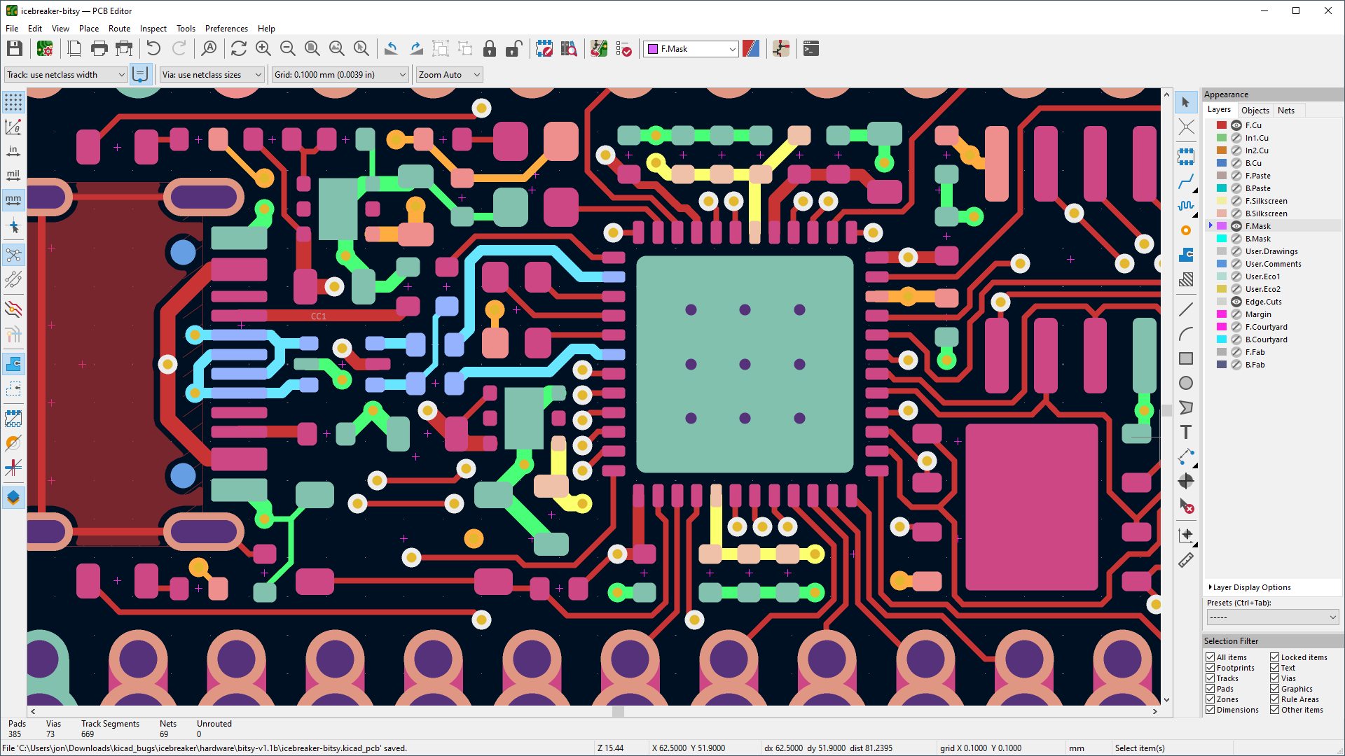
Source: https://www.kicad.org/img/frontpage/kicad_pcbnew.png
Evolution of PCB Design Tools
PCB design has come a long way. Back in the pre-2000s, engineers relied on manual drafting. So, they used tape, rulers, and hand-drawn layouts on clear film or paper. Understandably, it was slow and error-prone.
Then EDA software like early OrCAD, Protel, and Calay took over, adding basic schematics, auto-routing, and single-layer boards to computers.
Today, cloud-based AI tools like Altium 365 and Fusion 360 handle complex multi-layer designs with smart automation, signal analysis, and thermal checks. —a game-changer for grad students prototyping sensors and companies outsourcing PCB services.

The big shift is to collaborative platforms. Tools like Upverter offer real-time sharing with Git-like version control, so teams worldwide can edit, track changes, and merge designs without email ping-pong or file conflicts.
Thanks to these tools, prototyping cycles have reduced from weeks to days. Previously, multiple physical board spins now happen mostly in virtual simulations, which saves money, reduces waste, and speeds up IoT gadgets or EV projects to market fast.
Suggested Reading: Al Technology vs Electronic Design and Manufacturing
Key Features Driving Transformation
Modern PCB design tools are a mix of sophisticated technologies, driving the transformation in the manufacturing industry. Here are the key features of these tools:
AI-Powered Automation
AI-powered tools can now handle auto-routing, DRC (design rule checks), and smart component placement. They spot issues like spacing violations or bad traces early. For example, Ansys tools predict thermal hotspots before you build, saving rework.
Manufacturers and service providers prefer it for quick prototyping because it allows them to deliver error-free boards faster. Hence, there is no need for manual tweaks on dense designs, as AI does the heavy lifting, cutting hours of workflow.
Suggested Reading: How AI & Automation Are Transforming PCB Manufacturing
Cloud Collaboration and Libraries
Cloud platforms with shared libraries, like SnapEDA integration, cut errors in high-density boards. Access verified parts from anywhere—no digging for datasheets. Teams collaborate live, updating footprints together.
These tools are perfect for design teams who prefer sharing projects or companies outsourcing to global fabrications. One library update fixes everyone’s designs, speeding high-layer-count boards for 5G or wearables.
High-Speed Design Capabilities
Modern tools tackle impedance control, DDR routing, and EMI simulations for GHz signals. Set stackups, match lengths, and check reflections automatically. Great for grad students building fast sensor interfaces or industries doing EV power boards.
Service providers use these for compliant high-speed layouts. Go from schematic to passing eye diagram in one flow—no more post-fab signal fixes.
Recommended Reading: Avoid PCB Fab Errors: Why Your Fabrication Drawing is Critical
3D Modeling and Simulation
3D modeling integrates MCAD-ECAD workflows, like in Fusion 360, to check mechanical fit and signal integrity. These tools let you see how your board fits inside a case or phone before fabrication.
Manufacturers can run simulations for crosstalk or power delivery right in the tool. This helps designers test their PCB enclosures and industries avoid costly respins.

Source: medium.jpg (640×561)
Top Tools for Modern PCB Design
Modern PCB design tools are driving product development with advanced capabilities for schematic capture, layout, simulation, and manufacturability analysis. Here are some of the top tools used in the industry.
Altium Designer
Altium Designer is recognized for its powerful all-in-one environment, offering advanced routing, 3D PCB visualization, signal integrity analysis, and seamless collaboration between electrical and mechanical design teams. It is widely adopted in professional and high-complexity electronic product development.
KiCad
KiCad has gained significant popularity as a robust open-source PCB design suite. It provides schematic capture, PCB layout, 3D modeling, and simulation features, making it an excellent option for students, researchers, and professionals seeking flexibility without licensing costs.
KiCad
KiCad has gained significant popularity as a robust open-source PCB design suite. It provides schematic capture, PCB layout, 3D modeling, and simulation features, making it an excellent option for students, researchers, and professionals seeking flexibility without licensing costs.
EasyEDA
EasyEDA offers a cloud-based design platform that simplifies schematic design and PCB layout while integrating directly with fabrication services. Its accessibility and rapid prototyping support make it especially useful for hobbyists, startups, and educational use.
Autodesk Fusion
Autodesk Fusion combines electronics and mechanical design in a unified platform, enabling co-design workflows. This makes it particularly valuable in mechatronics, embedded product design, and projects requiring tight integration between PCB and enclosure development.
Cadence OrCAD
Cadence OrCAD remains a leading industry tool known for advanced simulation, constraint-driven design, and support for complex high-speed and multilayer PCB applications. It is widely used in professional environments where reliability and advanced analysis are essential.
Impact of Design Tools on Electronic Product Development
There are several ways in which the design tools have impacted product development. Inevitably, it has eased the production cycle for manufacturers. Here is how it’s impacting the industry.
Faster Time-to-Market
Tools like KiCad let Arduino and Raspberry Pi teams iterate on designs super fast. For example, open-source hackers used KiCad to prototype a Raspberry Pi HAT with EEPROMs, oscillators, and SMD parts in days—not weeks. They split schematics across sheets, ran external autorouters, and flipped to four layers easily.
A startup building a smart home IoT system with Arduino/ESP32 went from idea to working demo in under a month, beating rivals by launching first. This rapid cycle means quicker market entry for sensors or wearables.
Cost Reduction
Virtual prototyping cuts down physical board spins by 40%. Take an IoT sensor device case: A manufacturing firm prototyped predictive maintenance sensors on motors using edge computing sims first.
They tested data flows virtually, avoiding three costly fab runs. Digital twins caught assembly flaws early, cutting development costs 30-50%.
Enhanced Reliability
Predictive analytics automates IPC-2221 compliance for creepage in high-voltage PCBs. These tools can flag insulation gaps or voltage arcs before fab, using stackup calcs and sims. In an EV charger project, engineers caught a 500V creepage violation early, preventing field failures.
Ansys-like thermal predictions ensure hot spots don’t warp boards. Industries that want to outsource production can get DFM-ready designs, while students can build safe power sensors without lab mishaps.
Sustainability Gains
Optimizing trace lengths cuts power loss and material use. Short, wide traces drop resistance by 20% in battery IoT nodes, extending life. A wearable health monitor team trimmed copper by 15% via auto-routing, using less FR4 substrate. This means greener fabs with less waste.
For services, it lowers shipping weight; students prototype eco-friendly projects easily. These shifts let you focus on ideas, not grunt work—perfect for tight deadlines or budgets.
Challenges with PCB Design Tools
While there have been great advancements in PCB design tools, several challenges remain in their adoption and effective utilization. This section focuses on the key challenges with PCB design tools and how the future trends are likely to shape the PCB design industry.
Adaptation to New EDA Technology
One major hurdle is the learning curve associated with advanced electronic design automation (EDA) software. Modern tools offer powerful capabilities such as simulation, signal integrity analysis, 3D modeling, and AI-assisted routing, but mastering these features requires significant training and experience.
For students, new engineers, and even experienced designers transitioning from legacy platforms, this complexity can slow adoption and productivity.
Data Security
Particularly with the growing use of cloud-based design platforms, data security becomes a major concern for manufacturing companies. While cloud collaboration enables distributed engineering teams, version control, and remote access, it also raises concerns about intellectual property protection, cybersecurity risks, and data ownership.
For industries dealing with sensitive or proprietary designs, ensuring secure cloud infrastructure remains a critical concern. Integration with legacy systems also presents difficulties. Many organizations still rely on older CAD tools, databases, and manufacturing workflows that may not seamlessly interface with modern platforms, creating compatibility issues and resistance to migration.
Recommended Reading: From Prototype to Mass Production: Best Practices for Smooth NPI in PCB Design
Conclusion
Many experts predict that a substantial portion of PCB design tasks may become highly automated, potentially enabling mass customization in fields such as wearable electronics and edge AI devices. Designers may shift from manually executing routine tasks to supervising intelligent workflows and focusing on higher-level innovation.
In conclusion, while challenges such as steep learning curves, security concerns, and legacy integration remain, future trends point toward increasingly intelligent, connected, and automated design ecosystems. Ultimately, these tools empower engineers to spend less time on repetitive design tasks and more time driving innovation.
Frequently Asked Questions
1. How have PCB design tools improved electronic product development?
2. What is the evolution of PCB design tools?
3. What key features in modern PCB tools drive manufacturing transformation?
Features include DRC, DFM checks, signal integrity analysis, controlled impedance routing, thermal analysis, and automated manufacturing outputs.
4. Why are simulation and analysis tools important in PCB design?
They help detect issues early, optimize performance, reduce prototypes, and improve product reliability before manufacturing.
5. How do modern design tools support advanced technologies like IoT and high-speed electronics?
They provide multi-layer design support, high-speed routing, embedded system integration, and collaboration tools needed for complex modern products.
References
1.Global Market Insights, “Printed Circuit Board (PCB) Market Size to Surpass $120 Bn by 2030,” [Online]. Available: https://www.gminsights.com/pressrelease/printed-circuit-board-pcb-market
2.Altium Resources, “What is the Best PCB Design Tool For Students?,” [Online]. Available: https://resources.altium.com/p/what-best-pcb-design-tool-students
3.Printed Circuit Design & Fab, “PCB Design Industry Timeline,” [Online]. Available: https://www.pcdandf.com/pcdesign/index.php/menu-research/pcb-design-history/7736-pcb-design-industry-timeline
4.NCAB Group, “PCB design guidelines,” [Online]. Available: https://www.ncabgroup.com/pcb-design-guidelines/
5.Aivon, “AI-Powered PCB Design: How Machine Learning is Revolutionizing Layout in 2025,” [Online]. Available: https://www.aivon.com/blog/pcb-design/ai-powered-pcb-design-how-machine-learning-is-revolutionizing-layout-in-2025/
6.ProtoExpress, “10 Best PCB Layout Design Tools Recommended by PCB Designers,” [Online]. Available: https://www.protoexpress.com/blog/10-best-pcb-layout-design-tools-recommended-by-pcb-designers/
7.Rocket-PCB, “How to Design a PCB for High Frequency?,” [Online]. Available: https://www.rocket-pcb.com/how-to-design-a-pcb-for-high-frequency
8.Meegle, “Hardware Prototyping with Open-Source Tools,” [Online]. Available: https://www.meegle.com/en_us/topics/hardware-prototyping/hardware-prototyping-with-open-source-tools
9.Panasia Solutions, “IoT Device Prototyping: From Concept to Market,” [Online]. Available: https://panasia.solutions/iot-device-prototyping/


