
What is the PCB Lamination Process? Steps, Cycles & Common Defects
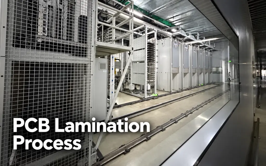
PCB lamination is a key step in multilayer PCB manufacturing process because separately patterned inner-layer circuits must be bonded into one board, with electrical insulation between the conductive layers. A conventional double-sided PCB, by contrast, has circuitry on the two faces of a single copper-clad laminate and normally does not require an additional multilayer lamination […]