
What Is PCB Layout? Definition, Process and Key Design Elements
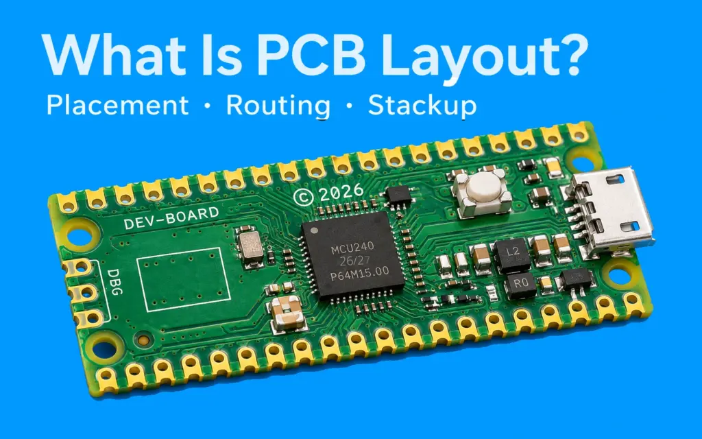
PCB layout turns a verified schematic or netlist into the physical arrangement and interconnection of a printed circuit board. It defines component footprints, placement, copper routing, vias, layer stackup, and mechanical boundaries.These decisions affect signal integrity, power delivery, thermal behavior, assembly, and manufacturing yield. A production-ready layout must meet electrical and mechanical requirements while staying […]