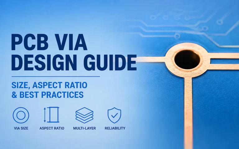
PCB Via Design Guide: Size, Aspect Ratio & Best Practices
Introduction A via may look like a simple hole in a PCB, but its drill diameter, pad diameter, annular ring, board thickness, plating, and layer transition all affect whether it

Introduction A via may look like a simple hole in a PCB, but its drill diameter, pad diameter, annular ring, board thickness, plating, and layer transition all affect whether it
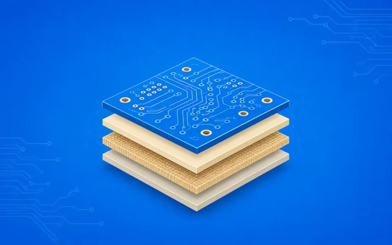
In PCB design and manufacturing, engineers usually focus on impedance control, thermal performance, stackup structure, and signal integrity. However, the base material itself determines another critical reliability factor: Comparative Tracking
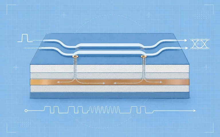
High-speed PCB design becomes necessary when the PCB interconnect starts to affect the voltage or timing seen by the receiver. There is no single clock-frequency threshold that tells you when
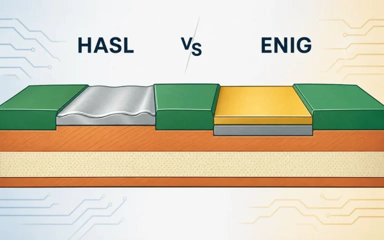
Lead-free HASL is usually the better starting point when cost matters and your assembly can tolerate some variation in pad height. ENIG becomes more useful when a flatter pad surface,

PCB manufacturing converts released design data into a tested bare circuit board through a controlled sequence of material transformation and verification steps. Each stage changes the board physically and must

PCB cost cannot be reduced to one reliable price per board, layer, or square inch. A bare-board quote depends on how the design uses a manufacturing panel, which process route
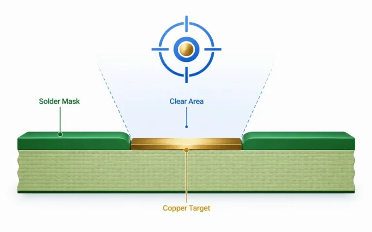
PCB fiducials are exposed copper reference marks used by SMT equipment to align the real board or panel with programmed CAD coordinates. Stencil printers and pick-and-place machines use them to
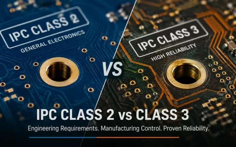
IPC Class 2 suits products that require long service life when temporary downtime and field repair remain acceptable. IPC Class 3 applies when operation on demand is critical, interruption creates
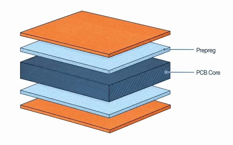
PCB core and prepreg are different material forms used for different functions in a multilayer stackup. A core is cured laminate, normally supplied with copper on both sides. Prepreg is
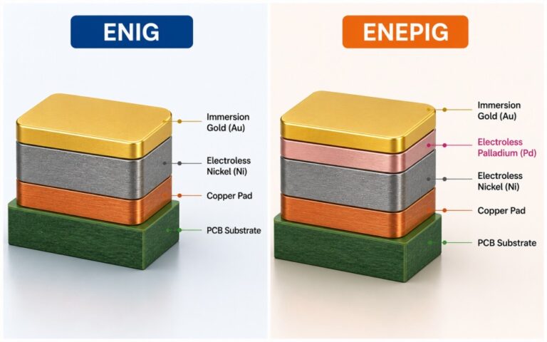
ENIG and ENEPIG are both flat, solderable PCB surface finishes. ENIG uses electroless nickel and immersion gold. ENEPIG adds an electroless palladium layer between the nickel and gold. In the
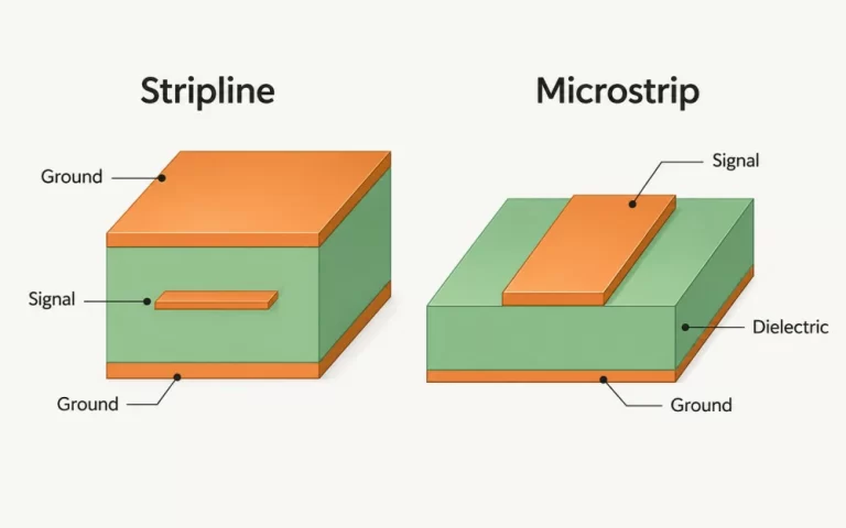
Neither structure wins every stripline vs microstrip comparison. Microstrip places the signal on an outer layer, which favors direct component launches, probing, and fewer layer transitions. Stripline embeds the signal
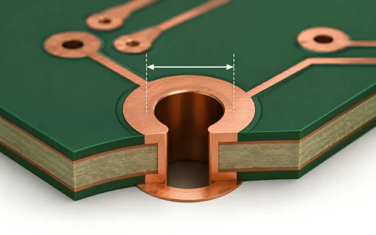
A PCB annular ring is the copper land between a drilled hole and the outer edge of its pad. For a centered circular pad and hole, the nominal radial width