
6-Layer PCB Stackup Design: Complete Guidelines for Optimal Performance
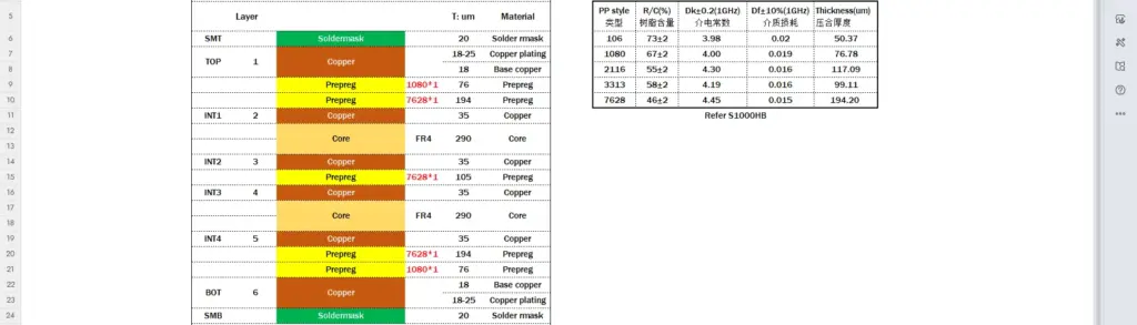
Our standard 6L PCB stack-up design options are suitable for most electronics design with upon global considerations of durable reliability, operation performance, economic cost and more available to PCB manufacturing process
4-Layer PCB Stackup Design: Complete Guidelines for Optimal Performance

Our standard 4L PCB stack-up design options are suitable for most electronics design with upon global considerations of durable reliability, operation performance, economic cost and more available to PCB manufacturing process
PCB Trace Width VS Current Value Calculator

While you start a PCB design, a typical PCB trace calculator will help you to get the correct copper weight and circuit trace width upon on the basic current that the board run.
Copper Pour in PCB Design: Fill Empty Areas for Better Manufacturing
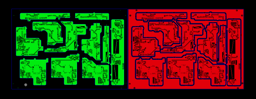
When electronic engineers create printed circuit boards (PCBs), they tend to leave many copper-free areas on the board. They are probably not aware of the technicalities of the PCB production process. A high percentage of the copper-free area on the board can have a negative impact on the product and leave it susceptible to early damage.