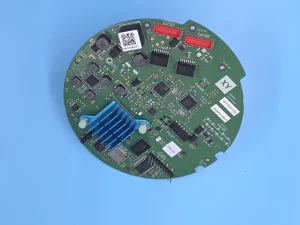
Xilinx Zynq-7000 XC7Z030-1FBG484C PCB Assembly
Core Advantages FPGA Device Xilinx Zynq-7000 XC7Z030-1FBG484C Package FBG484 (17mm


Core Advantages FPGA Device Xilinx Zynq-7000 XC7Z030-1FBG484C Package FBG484 (17mm
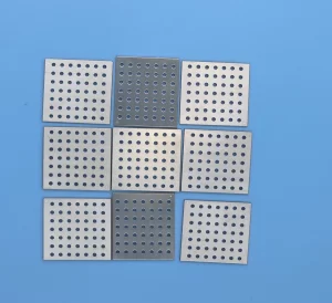
Core Advantages Material Nickel Silver (C7521), Tin-Plated Steel, or CuFe
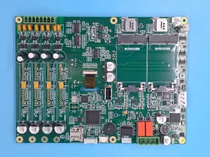
Core Advantages Fab & Assembly Standard IPC-A-610 Class 3 Inspection
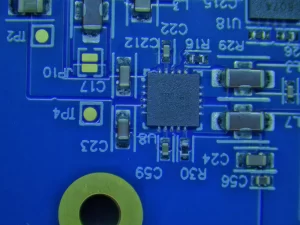
Core Advantages Fab & Assembly Standard IPC-A-610 Class 3 Inspection