
High Tg PCB: Benefits, Materials, Applications, and Design Guide
A High Tg PCB uses a laminate with a higher glass transition temperature than standard FR4. It resists heat better. It keeps its dimensions more
A High Tg PCB uses a laminate with a higher glass transition temperature than standard FR4. It resists heat better. It keeps its dimensions more
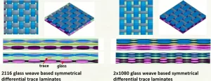
The glass fiber weave effect, also known as weave skew, is a critical signal integrity challenge in high-speed PCB design that occurs when differential pair
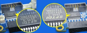
How to Spot Fake Electronic Component, The Dilemma We All Face If you run a small‑to‑medium volume electronics assembly line (or you entrust a small‑to‑medium
Electromagnetic interference (EMI) and electromagnetic compatibility (EMC) have become major concerns in modern industrial electronics. For instance, manufacturing plants, automation systems, robotics, motor drives, power
Printed circuit boards (PCBs) are found in almost every electronic product, such as phones, laptops, medical equipment, and factory machines. Understandably, testing of PCBs becomes

Printed circuit board or Printed wiring board is a core component in any electronics devices, such as FR4 PCB, Rogers PCB, High Tg PCB, impedance PCB…