
Essential PCB Layout Guidelines for High-Performance Electronics Design
In the world of electronics design, a schematic is only half the story. The true performance, reliability, and manufacturability of a product are determined during
In the world of electronics design, a schematic is only half the story. The true performance, reliability, and manufacturability of a product are determined during
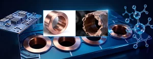
Copper electroplating is the backbone of modern printed circuit board (PCB) manufacturing. From through-hole connections in double-sided boards to microvias in HDI (High-Density Interconnect) structures,

Modern electronic systems are increasingly required to handle high voltages —from renewable energy converters and electric vehicles to medical imaging systems and industrial automation. Designing

The printed circuit board (PCB) manufacturing industry is undergoing a major transformation. As electronic products become smaller, faster, and more complex, traditional manufacturing methods are

In the electronics industry, building a working prototype is only the first step. The real challenge begins when that prototype must be converted into a
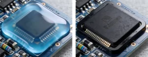
Conformal coating vs encapsulation for electronics is a critical decision for design engineers and product managers developing PCBs for harsh environments. Conformal coating applies a