HDI PCB Design, Manufacturing, Assembly, and Sourcing Guide
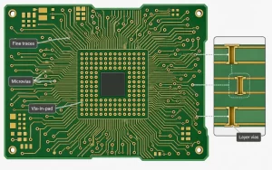
An HDI PCB is a high-density interconnect printed circuit board. It uses finer traces, smaller vias, and denser routing than a standard board. Most designs
An HDI PCB is a high-density interconnect printed circuit board. It uses finer traces, smaller vias, and denser routing than a standard board. Most designs
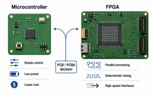
Choose a microcontroller when a product needs simple control, low power, lower cost, and fast firmware development. Choose an FPGA when the design needs parallel
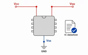
VCC and VDD usually mean the positive power rail. VSS usually means the lower power reference. In many simple CMOS circuits, VSS connects to GND.
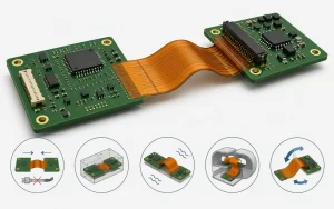
A rigid flex PCB is a packaging and reliability choice, not only a smaller way to connect two boards. Use it when cables, connectors, vibration,
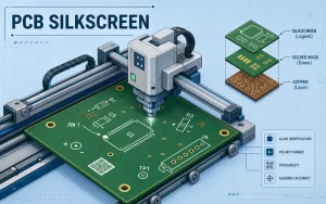
Silkscreen PCB is the printed legend layer that helps people read a circuit board during assembly, testing, repair, and traceability work. It is not just
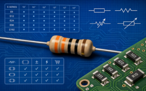
Resistor values affect current, voltage division, signal stability, heat, tolerance error, and long-term sourcing. A 10kΩ resistor may be a good GPIO pull-up, but the