
IPC Class 2 vs Class 3: Design, Verification, and Cost

IPC Class 2 suits products that require long service life when temporary downtime and field repair remain acceptable. IPC Class 3 applies when operation on demand is critical, interruption creates unacceptable consequences, or the product faces unusually harsh conditions.The selected class affects pad and hole geometry, registration margin, plated-hole control, inspection evidence, cost, and lead […]
PCB Prepreg vs Core: Differences, Stackup Use, and Verification

PCB core and prepreg are different material forms used for different functions in a multilayer stackup. A core is cured laminate, normally supplied with copper on both sides. Prepreg is a partially cured bonding material that flows and completes its cure during lamination. In practice, the design question is not which material is better. It […]
ENEPIG vs ENIG: Choose the Right PCB Surface Finish
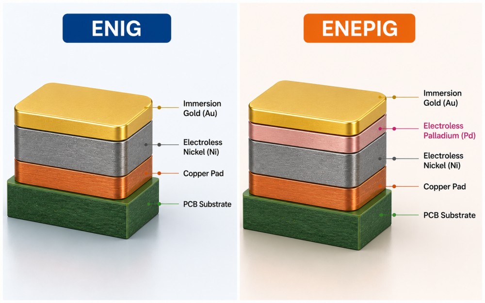
ENIG and ENEPIG are both flat, solderable PCB surface finishes. ENIG uses electroless nickel and immersion gold. ENEPIG adds an electroless palladium layer between the nickel and gold. In the ENEPIG vs ENIG decision, a controlled ENIG process is sufficient for many conventional SMT assemblies. ENEPIG becomes more useful when wire bonding, mixed interconnection methods, […]
Stripline vs Microstrip: PCB Stackup Selection Guide
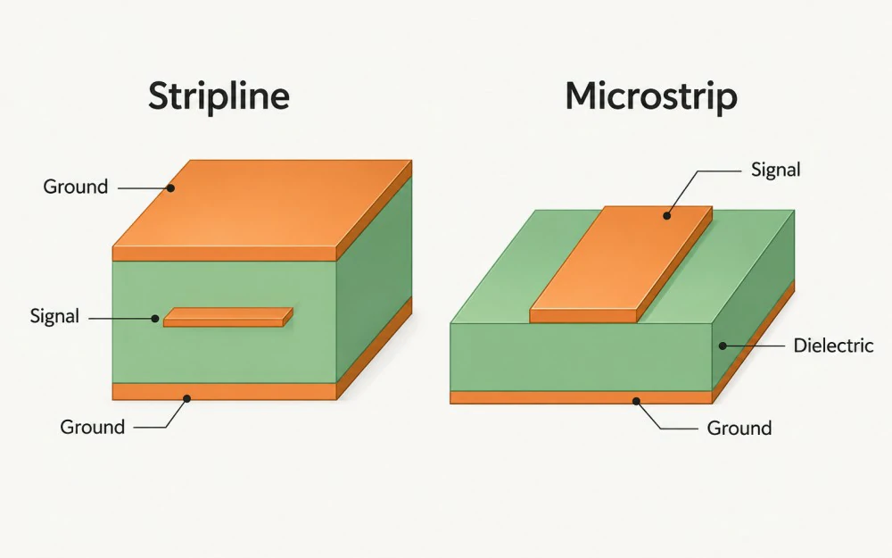
Neither structure wins every stripline vs microstrip comparison. Microstrip places the signal on an outer layer, which favors direct component launches, probing, and fewer layer transitions. Stripline embeds the signal between reference planes, which generally improves field containment when those references remain continuous.For a high-speed digital or RF path, start with the intended layer assignment […]
PCB Annular Ring Explained: Calculation, IPC & Breakout
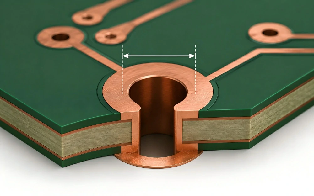
A PCB annular ring is the copper land between a drilled hole and the outer edge of its pad. For a centered circular pad and hole, the nominal radial width equals (pad diameter – hole diameter) / 2. This value describes ideal CAD geometry, not the minimum copper guaranteed on a finished board. Drill position, […]
Eye Diagram Analysis: Fix PCB Signal Integrity Problems
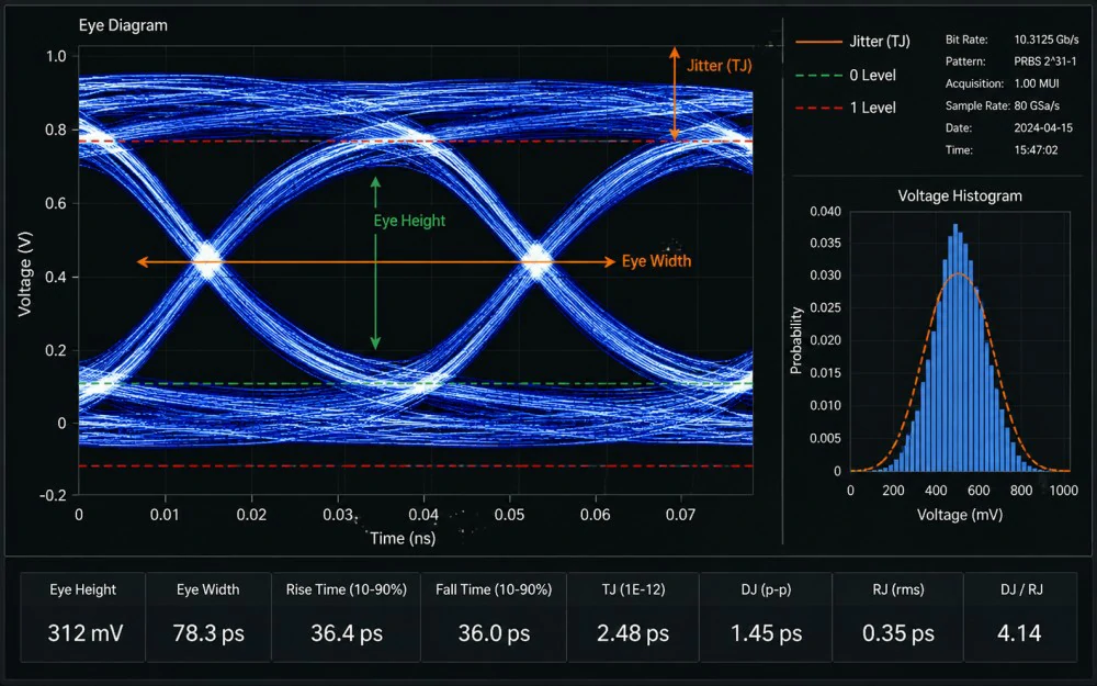
An eye diagram overlays repeated digital transitions to show voltage and timing margin at a selected measurement point. A wide, tall opening usually indicates a cleaner channel. Eye closure can suggest noise, jitter, loss, reflections, crosstalk, skew, or intersymbol interference.The eye shape does not identify the root cause alone. Engineers must connect the visible symptom […]